1. Power Distribution Network
2. Gigahertz Channel Design Considerations
3. PCB and Stack-Up Design Considerations
4. Device Pin-Map, Checklists, and Connection Guidelines
5. General Board Design Considerations/Guidelines
6. Memory Interfacing Guidelines
7. Power Dissipation and Thermal Management
8. Tools, Models, and Libraries
9. Reference Designs and Development Kits
10. Document Revision History for AN 958: Board Design Guidelines
4.1. High Speed Board Design Advisor
4.2. Complete Pin Connection Table by Device
4.3. Pin Connection Guidelines By Device
4.4. Design for Debug with JTAG Pins
4.5. Hot Socketing, POR and Power Sequencing Support
4.6. Implementing OCT
4.7. Unused I/O Pins Guidelines
4.8. Device Breakout Guidelines
4.9. Additional Resources
5.1.1. Material Selection and Loss
5.1.2. Cross Talk Minimization
5.1.3. Power Filtering/Distribution
5.1.4. Unused I/O Pins
5.1.5. Signal Trace Routing
5.1.6. Ground Bounce
5.1.7. Understanding Transmission Lines
5.1.8. Impedance Calculation
5.1.9. Coplanar Wave Guides
5.1.10. Simultaneous Switching Noise Guidelines
1.5.1. VRM
As a first-order approximation, the VRM can simply be modeled as a series connected resistor and inductor, as shown in Figure 2.
Figure 2. Series Impedance Model of a VRM
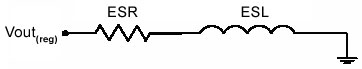
At low frequencies in the range of tens of KHz, the VRM, being primarily resistive, provides very low impedance and thus it is capable of providing the instantaneous current requirements at these lower frequencies. However, beyond a few tens of KHz, the VRM impedance being primarily inductive makes it incapable of providing the transient current requirements. You can get the ESR and ESL values of the VRM from the VRM manufacturer and you can choose a low ESR/ESL regulator for best transient performance.