1. Power Distribution Network
2. Gigahertz Channel Design Considerations
3. PCB and Stack-Up Design Considerations
4. Device Pin-Map, Checklists, and Connection Guidelines
5. General Board Design Considerations/Guidelines
6. Memory Interfacing Guidelines
7. Power Dissipation and Thermal Management
8. Tools, Models, and Libraries
9. Reference Designs and Development Kits
10. Document Revision History for AN 958: Board Design Guidelines
4.1. High Speed Board Design Advisor
4.2. Complete Pin Connection Table by Device
4.3. Pin Connection Guidelines By Device
4.4. Design for Debug with JTAG Pins
4.5. Hot Socketing, POR and Power Sequencing Support
4.6. Implementing OCT
4.7. Unused I/O Pins Guidelines
4.8. Device Breakout Guidelines
4.9. Additional Resources
5.1.1. Material Selection and Loss
5.1.2. Cross Talk Minimization
5.1.3. Power Filtering/Distribution
5.1.4. Unused I/O Pins
5.1.5. Signal Trace Routing
5.1.6. Ground Bounce
5.1.7. Understanding Transmission Lines
5.1.8. Impedance Calculation
5.1.9. Coplanar Wave Guides
5.1.10. Simultaneous Switching Noise Guidelines
1.5.3. Mounting Inductance
Mounting Inductance is the additional series inductance contribution associated with the mounting of the capacitor on the PCB. This parasitic inductance adds to the published ESL value that is provided by the cap vendor. Mounting inductance can be minimized by choosing smaller capacitor packages and performing proper layout of the capacitor on the PCB. Figure 3 shows the cross-section of a mounted decoupling capacitor in relation to the PCB planes and BGA device.
Figure 3. Decoupling Cap Mounting
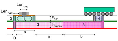
To estimate the mounting inductance, use the following equation:
- Lmnt = Ltrace + Lvia
Where,
- Ltrace = 128*[(2xLenpad)+Lencap]*(htop/w) pH
And,
- Lvia = 10*htop*ln(2s/D) ph
Where,
- Lenpad = Length of the capacitor pads plus trace length from pad to the via (mils)
- Lencap = Length of the capacitor body (mils)
- w = Width of the trace between the capacitor pad and via (mils)
- htop = Distance between the top layer and the nearest power/ground plane (mils)
- s = Distance between the capacitor's power via center and ground via center (mils)
- D = Outer diameter of the via (mils)
- hplanes = Distance between the power and ground plane (mils)
- b = Half the distance between the capacitor and the package power/ground vias (mils)
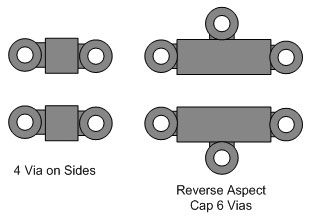
Generally, to minimize the mounting inductance, keep the capacitors power and ground vias as close as possible to its respective pad and use wide connecting traces and larger via drill diameters, if possible. Placing power and ground plane pairs closer to the surface where the capacitor is mounted reduces the via inductance contribution. Additionally, placing the vias on the same sides of the capacitor (via-on-side configuration) as opposed to the opposite ends of the capacitor (via-on-end configuration) reduces the current loop area, minimizing the amount of flux lines that penetrate the loop and thus reduces the inductance. Figure 4 illustrates the various capacitor layout topologies while Table 1 compares mounting inductance of those various cap layout styles for different size capacitors.
Figure 4. Various Capacitor Layout Topologies
| Via Length (height above plane, inches) |
0603 footprint |
0603 footprint |
0603 footprint |
0603 footprint |
0402 footprint |
0402 footprint |
|---|---|---|---|---|---|---|
| 0.020 drill | Thin trace from pad to via | Short thick trace | Via on the end of pads | Via on the side of pads | Via on the end of pads | Via on one side of pads |
| 0.004 | 1.57 | 1.04 | 0.82 | 0.52 | 0.8 | 0.5 |
| 0.006 | 1.96 | 1.35 | 1.05 | 0.65 | 1 | 0.63 |
| 0.01 | 2.51 | 1.87 | 1.4 | 0.88 | 1.34 | 0.86 |
| 0.02 | 3.45 | 2.87 | 2.13 | 1.39 | 1.99 | 1.36 |
| 0.010 drill | ||||||
| 0.004 | 1.61 | 1.08 | 0.86 | 0.56 | 0.84 | 0.54 |
| 0.006 | 1.99 | 1.39 | 1.08 | 0.69 | 1.04 | 0.67 |
| 0.01 | 2.55 | 1.92 | 1.45 | 0.92 | 1.38 | 0.9 |
| 0.02 | 3.49 | 2.91 | 2.17 | 1.44 | 2.03 | 1.4 |
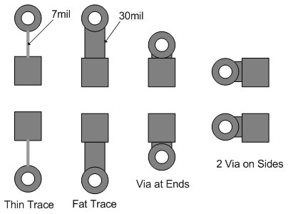
As shown in Table 1, the optimum mounting inductance of 0.50 nH is obtained when the smaller 0402 size capacitor is mounted using the via-on-side scheme with wide connecting traces to the larger 20 mil via drill diameter. Figure 5 shows other recommended via placement configurations that further reduce mounting inductance. However, these styles require additional vias and hampers routability.
Figure 5. Via placement Styles that Yield Lower Mounting Inductance