External Memory Interfaces (EMIF) IP User Guide: Agilex™ 5 FPGAs and SoCs
ID
817467
Date
3/31/2025
Public
A newer version of this document is available. Customers should click here to go to the newest version.
1. About the External Memory Interfaces Agilex™ 5 FPGA IP
2. Agilex™ 5 FPGA EMIF IP – Introduction
3. Agilex™ 5 FPGA EMIF IP – Product Architecture
4. Agilex™ 5 FPGA EMIF IP – End-User Signals
5. Agilex™ 5 FPGA EMIF IP – Simulating Memory IP
6. Agilex™ 5 FPGA EMIF IP - DDR4 Support
7. Agilex™ 5 FPGA EMIF IP - DDR5 Support
8. Agilex™ 5 FPGA EMIF IP - LPDDR4 Support
9. Agilex™ 5 FPGA EMIF IP - LPDDR5 Support
10. Agilex™ 5 FPGA EMIF IP – Timing Closure
11. Agilex™ 5 FPGA EMIF IP – Controller Optimization
12. Agilex™ 5 FPGA EMIF IP – Debugging
13. Agilex™ 5 FPGA EMIF IP - Mailbox Support
14. Document Revision History for External Memory Interfaces (EMIF) IP User Guide
3.2.1. Agilex™ 5 EMIF Architecture: I/O Subsystem
3.2.2. Agilex™ 5 EMIF Architecture: I/O SSM
3.2.3. Agilex™ 5 EMIF Architecture: HSIO Bank
3.2.4. Agilex™ 5 EMIF Architecture: I/O Lane
3.2.5. Agilex™ 5 EMIF Architecture: Input DQS Clock Tree
3.2.6. Agilex™ 5 EMIF Architecture: PHY Clock Tree
3.2.7. Agilex™ 5 EMIF Architecture: PLL Reference Clock Networks
3.2.8. Agilex™ 5 EMIF Architecture: Clock Phase Alignment
3.2.9. User Clock in Different Core Access Modes
4.1. IP Interfaces for Agilex 5 E-Series External Memory Interfaces (EMIF) IP - DDR4 Component
4.2. IP Interfaces for Agilex 5 E-Series External Memory Interfaces (EMIF) IP - DDR5 Component
4.3. IP Interfaces for Agilex 5 E-Series External Memory Interfaces (EMIF) IP - LPDDR4
4.4. IP Interfaces for Agilex 5 E-Series External Memory Interfaces (EMIF) IP - LPDDR5
4.1.1. s0_axi4_clock_in for Agilex 5 E-Series External Memory Interfaces (EMIF) IP - DDR4 Component
4.1.2. s0_axi4_clock_out for Agilex 5 E-Series External Memory Interfaces (EMIF) IP - DDR4 Component
4.1.3. s0_axi4_ctrl_ready for Agilex 5 E-Series External Memory Interfaces (EMIF) IP - DDR4 Component
4.1.4. core_init_n for Agilex 5 E-Series External Memory Interfaces (EMIF) IP - DDR4 Component
4.1.5. s0_axi4 for Agilex 5 E-Series External Memory Interfaces (EMIF) IP - DDR4 Component
4.1.6. s0_axi4lite_clock for Agilex 5 E-Series External Memory Interfaces (EMIF) IP - DDR4 Component
4.1.7. s0_axi4lite_reset_n for Agilex 5 E-Series External Memory Interfaces (EMIF) IP - DDR4 Component
4.1.8. s0_axi4lite for Agilex 5 E-Series External Memory Interfaces (EMIF) IP - DDR4 Component
4.1.9. mem_0 for Agilex 5 E-Series External Memory Interfaces (EMIF) IP - DDR4 Component
4.1.10. mem_ck_0 for Agilex 5 E-Series External Memory Interfaces (EMIF) IP - DDR4 Component
4.1.11. mem_reset_n for Agilex 5 E-Series External Memory Interfaces (EMIF) IP - DDR4 Component
4.1.12. oct_0 for Agilex 5 E-Series External Memory Interfaces (EMIF) IP - DDR4 Component
4.1.13. ref_clk for Agilex 5 E-Series External Memory Interfaces (EMIF) IP - DDR4 Component
4.2.1. s0_axi4_clock_in for Agilex 5 E-Series External Memory Interfaces (EMIF) IP - DDR5 Component
4.2.2. s0_axi4_clock_out for Agilex 5 E-Series External Memory Interfaces (EMIF) IP - DDR5 Component
4.2.3. s0_axi4_ctrl_ready for Agilex 5 E-Series External Memory Interfaces (EMIF) IP - DDR5 Component
4.2.4. core_init_n for Agilex 5 E-Series External Memory Interfaces (EMIF) IP - DDR5 Component
4.2.5. s0_axi4 for Agilex 5 E-Series External Memory Interfaces (EMIF) IP - DDR5 Component
4.2.6. s1_axi4 for Agilex 5 E-Series External Memory Interfaces (EMIF) IP - DDR5 Component
4.2.7. s0_axi4lite_clock for Agilex 5 E-Series External Memory Interfaces (EMIF) IP - DDR5 Component
4.2.8. s0_axi4lite_reset_n for Agilex 5 E-Series External Memory Interfaces (EMIF) IP - DDR5 Component
4.2.9. s0_axi4lite for Agilex 5 E-Series External Memory Interfaces (EMIF) IP - DDR5 Component
4.2.10. mem_0 for Agilex 5 E-Series External Memory Interfaces (EMIF) IP - DDR5 Component
4.2.11. mem_ck_0 for Agilex 5 E-Series External Memory Interfaces (EMIF) IP - DDR5 Component
4.2.12. mem_reset_n_0 for Agilex 5 E-Series External Memory Interfaces (EMIF) IP - DDR5 Component
4.2.13. mem_1 for Agilex 5 E-Series External Memory Interfaces (EMIF) IP - DDR5 Component
4.2.14. mem_ck_1 for Agilex 5 E-Series External Memory Interfaces (EMIF) IP - DDR5 Component
4.2.15. mem_reset_n_1 for Agilex 5 E-Series External Memory Interfaces (EMIF) IP - DDR5 Component
4.2.16. oct_0 for Agilex 5 E-Series External Memory Interfaces (EMIF) IP - DDR5 Component
4.2.17. oct_1 for Agilex 5 E-Series External Memory Interfaces (EMIF) IP - DDR5 Component
4.2.18. ref_clk for Agilex 5 E-Series External Memory Interfaces (EMIF) IP - DDR5 Component
4.3.1. s0_axi4_clock_in for Agilex 5 E-Series External Memory Interfaces (EMIF) IP - LPDDR4
4.3.2. core_init_n for Agilex 5 E-Series External Memory Interfaces (EMIF) IP - LPDDR4
4.3.3. s0_axi4_ctrl_ready for Agilex 5 E-Series External Memory Interfaces (EMIF) IP - LPDDR4
4.3.4. s0_axi4_clock_out for Agilex 5 E-Series External Memory Interfaces (EMIF) IP - LPDDR4
4.3.5. s1_axi4_ctrl_ready for Agilex 5 E-Series External Memory Interfaces (EMIF) IP - LPDDR4
4.3.6. s1_axi4_clock_out for Agilex 5 E-Series External Memory Interfaces (EMIF) IP - LPDDR4
4.3.7. s0_axi4 for Agilex 5 E-Series External Memory Interfaces (EMIF) IP - LPDDR4
4.3.8. s1_axi4 for Agilex 5 E-Series External Memory Interfaces (EMIF) IP - LPDDR4
4.3.9. s2_axi4 for Agilex 5 E-Series External Memory Interfaces (EMIF) IP - LPDDR4
4.3.10. s3_axi4 for Agilex 5 E-Series External Memory Interfaces (EMIF) IP - LPDDR4
4.3.11. s0_axi4lite_clock for Agilex 5 E-Series External Memory Interfaces (EMIF) IP - LPDDR4
4.3.12. s0_axi4lite_reset_n for Agilex 5 E-Series External Memory Interfaces (EMIF) IP - LPDDR4
4.3.13. s0_axi4lite for Agilex 5 E-Series External Memory Interfaces (EMIF) IP - LPDDR4
4.3.14. s1_axi4lite_clock for Agilex 5 E-Series External Memory Interfaces (EMIF) IP - LPDDR4
4.3.15. s1_axi4lite_reset_n for Agilex 5 E-Series External Memory Interfaces (EMIF) IP - LPDDR4
4.3.16. s1_axi4lite for Agilex 5 E-Series External Memory Interfaces (EMIF) IP - LPDDR4
4.3.17. mem_0 for Agilex 5 E-Series External Memory Interfaces (EMIF) IP - LPDDR4
4.3.18. mem_ck_0 for Agilex 5 E-Series External Memory Interfaces (EMIF) IP - LPDDR4
4.3.19. mem_1 for Agilex 5 E-Series External Memory Interfaces (EMIF) IP - LPDDR4
4.3.20. mem_ck_1 for Agilex 5 E-Series External Memory Interfaces (EMIF) IP - LPDDR4
4.3.21. mem_2 for Agilex 5 E-Series External Memory Interfaces (EMIF) IP - LPDDR4
4.3.22. mem_ck_2 for Agilex 5 E-Series External Memory Interfaces (EMIF) IP - LPDDR4
4.3.23. mem_3 for Agilex 5 E-Series External Memory Interfaces (EMIF) IP - LPDDR4
4.3.24. mem_ck_3 for Agilex 5 E-Series External Memory Interfaces (EMIF) IP - LPDDR4
4.3.25. mem_reset_n for Agilex 5 E-Series External Memory Interfaces (EMIF) IP - LPDDR4
4.3.26. oct_0 for Agilex 5 E-Series External Memory Interfaces (EMIF) IP - LPDDR4
4.3.27. oct_1 for Agilex 5 E-Series External Memory Interfaces (EMIF) IP - LPDDR4
4.3.28. oct_2 for Agilex 5 E-Series External Memory Interfaces (EMIF) IP - LPDDR4
4.3.29. oct_3 for Agilex 5 E-Series External Memory Interfaces (EMIF) IP - LPDDR4
4.3.30. ref_clk for Agilex 5 E-Series External Memory Interfaces (EMIF) IP - LPDDR4
4.4.1. s0_axi4_clock_in for Agilex 5 E-Series External Memory Interfaces (EMIF) IP - LPDDR5
4.4.2. core_init_n for Agilex 5 E-Series External Memory Interfaces (EMIF) IP - LPDDR5
4.4.3. s0_axi4_ctrl_ready for Agilex 5 E-Series External Memory Interfaces (EMIF) IP - LPDDR5
4.4.4. s0_axi4_clock_out for Agilex 5 E-Series External Memory Interfaces (EMIF) IP - LPDDR5
4.4.5. s1_axi4_ctrl_ready for Agilex 5 E-Series External Memory Interfaces (EMIF) IP - LPDDR5
4.4.6. s1_axi4_clock_out for Agilex 5 E-Series External Memory Interfaces (EMIF) IP - LPDDR5
4.4.7. s0_axi4 for Agilex 5 E-Series External Memory Interfaces (EMIF) IP - LPDDR5
4.4.8. s1_axi4 for Agilex 5 E-Series External Memory Interfaces (EMIF) IP - LPDDR5
4.4.9. s2_axi4 for Agilex 5 E-Series External Memory Interfaces (EMIF) IP - LPDDR5
4.4.10. s3_axi4 for Agilex 5 E-Series External Memory Interfaces (EMIF) IP - LPDDR5
4.4.11. s0_axi4lite_clock for Agilex 5 E-Series External Memory Interfaces (EMIF) IP - LPDDR5
4.4.12. s0_axi4lite_reset_n for Agilex 5 E-Series External Memory Interfaces (EMIF) IP - LPDDR5
4.4.13. s0_axi4lite for Agilex 5 E-Series External Memory Interfaces (EMIF) IP - LPDDR5
4.4.14. s1_axi4lite_clock for Agilex 5 E-Series External Memory Interfaces (EMIF) IP - LPDDR5
4.4.15. s1_axi4lite_reset_n for Agilex 5 E-Series External Memory Interfaces (EMIF) IP - LPDDR5
4.4.16. s1_axi4lite for Agilex 5 E-Series External Memory Interfaces (EMIF) IP - LPDDR5
4.4.17. mem_0 for Agilex 5 E-Series External Memory Interfaces (EMIF) IP - LPDDR5
4.4.18. mem_ck_0 for Agilex 5 E-Series External Memory Interfaces (EMIF) IP - LPDDR5
4.4.19. mem_1 for Agilex 5 E-Series External Memory Interfaces (EMIF) IP - LPDDR5
4.4.20. mem_ck_1 for Agilex 5 E-Series External Memory Interfaces (EMIF) IP - LPDDR5
4.4.21. mem_2 for Agilex 5 E-Series External Memory Interfaces (EMIF) IP - LPDDR5
4.4.22. mem_ck_2 for Agilex 5 E-Series External Memory Interfaces (EMIF) IP - LPDDR5
4.4.23. mem_3 for Agilex 5 E-Series External Memory Interfaces (EMIF) IP - LPDDR5
4.4.24. mem_ck_3 for Agilex 5 E-Series External Memory Interfaces (EMIF) IP - LPDDR5
4.4.25. mem_reset_n for Agilex 5 E-Series External Memory Interfaces (EMIF) IP - LPDDR5
4.4.26. oct_0 for Agilex 5 E-Series External Memory Interfaces (EMIF) IP - LPDDR5
4.4.27. oct_1 for Agilex 5 E-Series External Memory Interfaces (EMIF) IP - LPDDR5
4.4.28. oct_2 for Agilex 5 E-Series External Memory Interfaces (EMIF) IP - LPDDR5
4.4.29. oct_3 for Agilex 5 E-Series External Memory Interfaces (EMIF) IP - LPDDR5
4.4.30. ref_clk for Agilex 5 E-Series External Memory Interfaces (EMIF) IP - LPDDR5
6.3.3.1. Address and Command Pin Placement for DDR4
6.3.3.2. DDR4 Data Width Mapping
6.3.3.3. Clamshell Topology
6.3.3.4. General Guidelines
6.3.3.5. x4 DIMM Implementation
6.3.3.6. Specific Pin Connection Requirements
6.3.3.7. Command and Address Signals
6.3.3.8. Clock Signals
6.3.3.9. Data, Data Strobes, DM/DBI, and Optional ECC Signals
12.1. Interface Configuration Performance Issues
12.2. Functional Issue Evaluation
12.3. Timing Issue Characteristics
12.4. Verifying Memory IP Using the Signal Tap Logic Analyzer
12.5. Debugging with the External Memory Interface Debug Toolkit
12.6. Generating Traffic with the Test Engine IP
12.7. Guidelines for Developing HDL for Traffic Generator
12.8. Guidelines for Traffic Generator Status Check
12.9. Hardware Debugging Guidelines
12.10. Categorizing Hardware Issues
12.9.1. Create a Simplified Design that Demonstrates the Same Issue
12.9.2. Measure Power Distribution Network
12.9.3. Measure Signal Integrity and Setup and Hold Margin
12.9.4. Vary Voltage
12.9.5. Operate at a Lower Speed
12.9.6. Determine Whether the Issue Exists in Previous Versions of Software
12.9.7. Determine Whether the Issue Exists in the Current Version of Software
12.9.8. Try A Different PCB
12.9.9. Try Other Configurations
12.9.10. Debugging Checklist
12.10.1.1. Characteristics of Signal Integrity Issues
12.10.1.2. Evaluating Signal Integrity Issues
12.10.1.3. Skew
12.10.1.4. Crosstalk
12.10.1.5. Power System
12.10.1.6. Clock Signals
12.10.1.7. Address and Command Signals
12.10.1.8. Read Data Valid Window and Eye Diagram
12.10.1.9. Write Data Valid Window and Eye Diagram
- 4.1.2. s0_axi4_clock_out for Agilex 5 E-Series External Memory Interfaces (EMIF) IP - DDR4 Component
- 4.2.2. s0_axi4_clock_out for Agilex 5 E-Series External Memory Interfaces (EMIF) IP - DDR5 Component
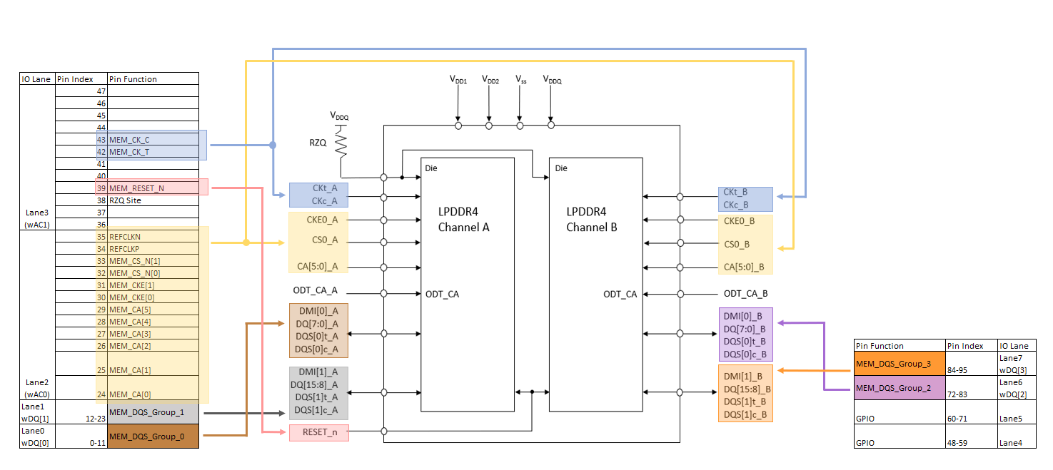
8.2.3.6. LPDDR4 Data Width Mapping
Agilex™ 5 FPGA LPDDR4 IP supports fixed address and command pin placement, and fixed data lanes placement.
You can only use fixed byte lanes within the I/O Bank as data lanes. Below is the summary of the location for address and command, and data lanes.
For two-channel x16 LPDDR4, the DQ group placement must follow the controller I/O sub-bank:
| Controller | Data Width | BL7 [P95:P84] | BL6 [P83:P72] | BL5 [P71:P60] | BL4 [P59:P48] | BL3 [P47:P36] | BL2 [P35:P24] | BL1 [P23:P12] | BL0 [P11:P0] | BL7 [P95:P84] | BL6 [P83:P72] | BL5 [P71:P60] | BL4 [P59:P48] | BL3 [P47:P36] | BL2 [P35:P24] | BL1 [P23:P12] | BL0 [P11:P0] | |
|---|---|---|---|---|---|---|---|---|---|---|---|---|---|---|---|---|---|---|
| Primary | LPDDR4 x32 | DQ[3] P | DQ[2] P | GPIO | GPIO | AC1 P | AC0 P | DQ[1] P | DQ[0] P | |||||||||
| Primary | LPDDR4 1ch x16 | GPIO | GPIO | GPIO | GPIO | AC1 P | AC0 P | wDQ[1] | wDQ[0] | |||||||||
| Primary + Secondary | LPDDR4 2ch x16 | DQ[1] S | DQ[0] S | AC1 S | AC0 S | AC1 P | AC0- P | DQ[1] P | DQ[0] P | |||||||||
| Primary + Secondary | LPDDR4 4ch x16 | DQ[1] S | DQ[0] S | AC1 S | AC0 S | AC1 P | AC0- P | DQ[1] P | DQ[0] P | DQ[1] S | DQ[0] S | AC1 S | AC0 S | AC1 P | AC0 P | DQ[1] P | DQ[0] P | |
|
Note:
|
||||||||||||||||||
The diagrams below illustrates the pin connections for address and command and the data group.
Note: Refer to the LPDDR4 pin table in the Product Architecture chapter for detailed pin placement for both address and command and DQ pins.
Figure 27. Dual-Channel x16 LPDDR4, Single Rank
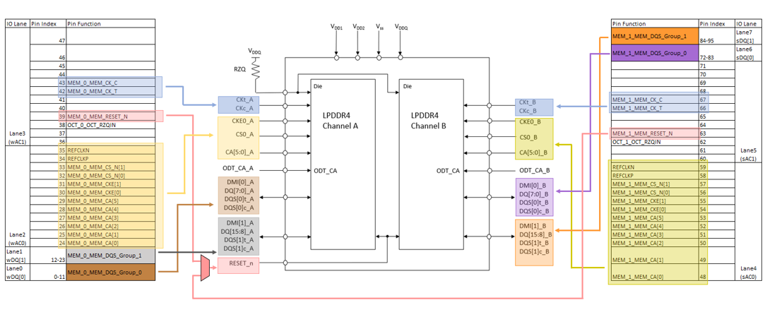
Figure 28. Single-Channel x32 LPDDR4, Single Rank