External Memory Interfaces (EMIF) IP User Guide: Agilex™ 5 FPGAs and SoCs
A newer version of this document is available. Customers should click here to go to the newest version.
- 4.1.2. s0_axi4_clock_out for Agilex 5 E-Series External Memory Interfaces (EMIF) IP - DDR4 Component
- 4.2.2. s0_axi4_clock_out for Agilex 5 E-Series External Memory Interfaces (EMIF) IP - DDR5 Component
6.3.3.3. Clamshell Topology
In a DDR4 clamshell topology, SDRAM is arranged in two layers along either side of the chip, with individual memory devices opposite one another. This configuration allows for a smaller footprint than with fly-by topology, where memory devices are arranged on a single layer.
(Clamshell topology is not supported on the following ES0 devices: A5EX065BB23AEXSR0, A5EX065BB32AEXSR0, A5EX013BB23AEXSR0.)
The small footprint of the clamshell topology requires less board space than fly-by topology; however, the close proximity of the memory devices in clamshell topology increases the complexity of the required device routing to prevent signal integrity problems. Clamshell topology uses Address Mirroring to minimize undesired effects such as cross-talk, by splitting the chip select signal for each rank, as follows:
- A chip select that accesses the top layer of components, which have not been mirrored.
- A chip select that accesses the bottom layer of components, which have been mirrored.
The total number of chip selects required is double the interface's rank — for example, a single-rank memory interface requires two chip selects. The two chip selects are required for proper calibration of the interface, as a means of accounting for address mirroring. DDR4 component EMIF IP on Agilex™ 5 devices can support only single rank in clamshell topology.
The JEDEC specification JESD21-C defines address mirroring for DDR4 as shown in the table below:
| Memory Controller Pin | DRAM Pin (Non-mirrored) | DRAM Pin (Mirrored) |
|---|---|---|
| A3 | A3 | A4 |
| A4 | A4 | A3 |
| A5 | A5 | A6 |
| A6 | A6 | A5 |
| A7 | A7 | A8 |
| A8 | A8 | A7 |
| A11 | A11 | A13 |
| A13 | A13 | A11 |
| BA0 | BA0 | BA1 |
| BA1 | BA1 | BA0 |
| BG0 1 | BG0 | BG1 |
| BG1 1 | BG1 | BG0 |
| 1 BG0 and BG1 can be mirrored only when BG1 is present on the memory device. | ||
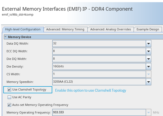
Enabling Clamshell Topology in Your External Memory Interface
- Configure a single memory interface according to your requirements.
- Enable Use Clamshell Topology on the Memory Device section on the High-level Configuration tab.
| Rank | Top/Bottom of Memory Device | CS Pin on Memory Device | CS Pin on FPGA |
|---|---|---|---|
| 0 | Top | CS0 | CS0 |
| 0 | Bottom | CS0 | CS1 |