External Memory Interfaces Cyclone® 10 GX FPGA IP User Guide
ID
683663
Date
11/28/2024
Public
1. Release Information
2. External Memory Interfaces Cyclone® 10 GX FPGA IP Introduction
3. Cyclone® 10 GX EMIF IP Product Architecture
4. Cyclone® 10 GX EMIF IP End-User Signals
5. Cyclone® 10 GX EMIF – Simulating Memory IP
6. Cyclone® 10 GX EMIF IP for DDR3
7. Cyclone® 10 GX EMIF IP for LPDDR3
8. Cyclone® 10 GX EMIF IP Timing Closure
9. Optimizing Controller Performance
10. Cyclone® 10 GX EMIF IP Debugging
11. External Memory Interfaces Cyclone® 10 GX FPGA IP User Guide Archives
12. Document Revision History for Cyclone® 10 GX External Memory Interfaces FPGA IP User Guide
4.1.1.1. pll_ref_clk for DDR3
4.1.1.2. pll_locked for DDR3
4.1.1.3. pll_extra_clk_0 for DDR3
4.1.1.4. pll_extra_clk_1 for DDR3
4.1.1.5. pll_extra_clk_2 for DDR3
4.1.1.6. pll_extra_clk_3 for DDR3
4.1.1.7. oct for DDR3
4.1.1.8. mem for DDR3
4.1.1.9. status for DDR3
4.1.1.10. afi_reset_n for DDR3
4.1.1.11. afi_clk for DDR3
4.1.1.12. afi_half_clk for DDR3
4.1.1.13. afi for DDR3
4.1.1.14. emif_usr_reset_n for DDR3
4.1.1.15. emif_usr_clk for DDR3
4.1.1.16. emif_usr_reset_n_sec for DDR3
4.1.1.17. emif_usr_clk_sec for DDR3
4.1.1.18. cal_debug_reset_n for DDR3
4.1.1.19. cal_debug_clk for DDR3
4.1.1.20. cal_debug_out_reset_n for DDR3
4.1.1.21. cal_debug_out_clk for DDR3
4.1.1.22. clks_sharing_master_out for DDR3
4.1.1.23. clks_sharing_slave_in for DDR3
4.1.1.24. clks_sharing_slave_out for DDR3
4.1.1.25. ctrl_amm for DDR3
4.1.1.26. ctrl_auto_precharge for DDR3
4.1.1.27. ctrl_user_priority for DDR3
4.1.1.28. ctrl_ecc_user_interrupt for DDR3
4.1.1.29. ctrl_ecc_readdataerror for DDR3
4.1.1.30. ctrl_mmr_slave for DDR3
4.1.1.31. cal_debug for DDR3
4.1.1.32. cal_debug_out for DDR3
4.1.2.1. pll_ref_clk for LPDDR3
4.1.2.2. pll_locked for LPDDR3
4.1.2.3. pll_extra_clk_0 for LPDDR3
4.1.2.4. pll_extra_clk_1 for LPDDR3
4.1.2.5. pll_extra_clk_2 for LPDDR3
4.1.2.6. pll_extra_clk_3 for LPDDR3
4.1.2.7. oct for LPDDR3
4.1.2.8. mem for LPDDR3
4.1.2.9. status for LPDDR3
4.1.2.10. afi_reset_n for LPDDR3
4.1.2.11. afi_clk for LPDDR3
4.1.2.12. afi_half_clk for LPDDR3
4.1.2.13. afi for LPDDR3
4.1.2.14. emif_usr_reset_n for LPDDR3
4.1.2.15. emif_usr_clk for LPDDR3
4.1.2.16. cal_debug_reset_n for LPDDR3
4.1.2.17. cal_debug_clk for LPDDR3
4.1.2.18. cal_debug_out_reset_n for LPDDR3
4.1.2.19. cal_debug_out_clk for LPDDR3
4.1.2.20. clks_sharing_master_out for LPDDR3
4.1.2.21. clks_sharing_slave_in for LPDDR3
4.1.2.22. clks_sharing_slave_out for LPDDR3
4.1.2.23. ctrl_user_priority for LPDDR3
4.1.2.24. ctrl_mmr_slave for LPDDR3
4.1.2.25. cal_debug for LPDDR3
4.1.2.26. cal_debug_out for LPDDR3
4.4.1. ctrlcfg0
4.4.2. ctrlcfg1
4.4.3. dramtiming0
4.4.4. sbcfg1
4.4.5. caltiming0
4.4.6. caltiming1
4.4.7. caltiming2
4.4.8. caltiming3
4.4.9. caltiming4
4.4.10. caltiming9
4.4.11. dramaddrw
4.4.12. sideband0
4.4.13. sideband1
4.4.14. sideband2
4.4.15. sideband3
4.4.16. sideband4
4.4.17. sideband5
4.4.18. sideband6
4.4.19. sideband7
4.4.20. sideband8
4.4.21. sideband9
4.4.22. sideband10
4.4.23. sideband11
4.4.24. sideband12
4.4.25. sideband13
4.4.26. dramsts
4.4.27. niosreserve0
4.4.28. niosreserve1
4.4.29. ecc3: ECC Error and Interrupt Configuration
4.4.30. ecc4: Status and Error Information
4.4.31. ecc5: Address of Most Recent SBE/DBE
4.4.32. ecc6: Address of Most Recent Correction Command Dropped
6.1.1. Intel Cyclone 10 GX EMIF IP DDR3 Parameters: General
6.1.2. Intel Cyclone 10 GX EMIF IP DDR3 Parameters: Memory
6.1.3. Intel Cyclone 10 GX EMIF IP DDR3 Parameters: Mem I/O
6.1.4. Intel Cyclone 10 GX EMIF IP DDR3 Parameters: FPGA I/O
6.1.5. Intel Cyclone 10 GX EMIF IP DDR3 Parameters: Mem Timing
6.1.6. Intel Cyclone 10 GX EMIF IP DDR3 Parameters: Board
6.1.7. Intel Cyclone 10 GX EMIF IP DDR3 Parameters: Controller
6.1.8. Intel Cyclone 10 GX EMIF IP DDR3 Parameters: Diagnostics
6.1.9. Intel Cyclone 10 GX EMIF IP DDR3 Parameters: Example Designs
7.1.1. Intel Cyclone 10 GX EMIF IP LPDDR3 Parameters: General
7.1.2. Intel Cyclone 10 GX EMIF IP LPDDR3 Parameters: Memory
7.1.3. Intel Cyclone 10 GX EMIF IP LPDDR3 Parameters: Mem I/O
7.1.4. Intel Cyclone 10 GX EMIF IP LPDDR3 Parameters: FPGA I/O
7.1.5. Intel Cyclone 10 GX EMIF IP LPDDR3 Parameters: Mem Timing
7.1.6. Intel Cyclone 10 GX EMIF IP LPDDR3 Parameters: Board
7.1.7. Intel Cyclone 10 GX EMIF IP LPDDR3 Parameters: Controller
7.1.8. Intel Cyclone 10 GX EMIF IP LPDDR3 Parameters: Diagnostics
7.1.9. Intel Cyclone 10 GX EMIF IP LPDDR3 Parameters: Example Designs
9.4.1. Auto-Precharge Commands
9.4.2. Latency
9.4.3. Calibration
9.4.4. Bank Interleaving
9.4.5. Additive Latency and Bank Interleaving
9.4.6. User-Controlled Refresh
9.4.7. Frequency of Operation
9.4.8. Series of Reads or Writes
9.4.9. Data Reordering
9.4.10. Starvation Control
9.4.11. Command Reordering
9.4.12. Bandwidth
9.4.13. Enable Command Priority Control
10.1. Interface Configuration Performance Issues
10.2. Functional Issue Evaluation
10.3. Timing Issue Characteristics
10.4. Verifying Memory IP Using the Signal Tap II Logic Analyzer
10.5. Hardware Debugging Guidelines
10.6. Categorizing Hardware Issues
10.7. Debugging Cyclone® 10 GX EMIF IP
10.8. Using the Traffic Generator with the Generated Design Example
10.5.1. Create a Simplified Design that Demonstrates the Same Issue
10.5.2. Measure Power Distribution Network
10.5.3. Measure Signal Integrity and Setup and Hold Margin
10.5.4. Vary Voltage
10.5.5. Operate at a Lower Speed
10.5.6. Determine Whether the Issue Exists in Previous Versions of Software
10.5.7. Determine Whether the Issue Exists in the Current Version of Software
10.5.8. Try A Different PCB
10.5.9. Try Other Configurations
10.5.10. Debugging Checklist
3.4.1. Hard Memory Controller
The Cyclone® 10 hard memory controller is designed for high speed, high performance, high flexibility, and area efficiency. The Cyclone® 10 hard memory controller supports DDR3 and LPDDR3 memory standards.
The hard memory controller implements efficient pipelining techniques and advanced dynamic command and data reordering algorithms to improve bandwidth usage and reduce latency, providing a high performance solution.
The controller architecture is modular and fits in a single I/O bank. The structure allows you to:
- Configure each I/O bank as either:
- A control path that drives all the address and command pins for the memory interface.
- A data path that drives up to 32 data pins for DDR-type interfaces.
- Place your memory controller in any location.
- Pack up multiple banks together to form memory interfaces of different widths up to 144 bits.
- Bypass the hard memory controller and use your own custom IP if required.
Figure 15. Hard Memory Controller Architecture
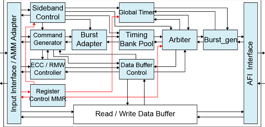
The hard memory controller consists of the following logic blocks:
- Core and PHY interfaces
- Main control path
- Data buffer controller
- Read and write data buffers
The core interface supports the Avalon® Memory-Mapped (Avalon-MM) interface. The interface communicates to the PHY using the Altera PHY Interface (AFI). The whole control path is split into the main control path and the data buffer controller.