AN 773: Drive-On-Chip Design Example for Intel® MAX® 10 Devices
7.9.1.1. DC-DC Control Block
The DC-DC control block consists of
- Fault latches block
- PI controller block
- Two independent current control loops
- Voltage control loop
- PWM block
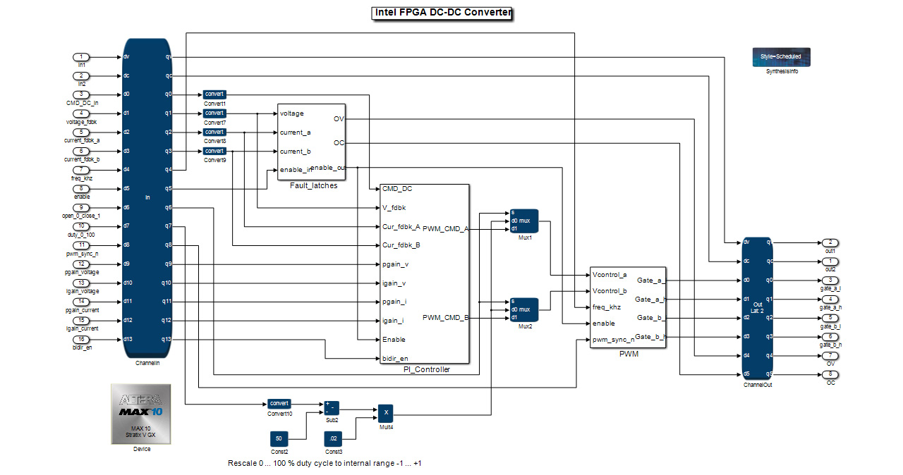
The DC-DC control block has the portion of the simulation for which you generate VHDL code. The ChannelIn and ChannelOut blocks are the port interface for the VHDL code. The MATLAB Simulink* inport and output signals define the VHDL signal names, and the VHDL data formats are the signal formats that you typically set with the Convert block.
The Convert DSP block sets the data format. This model uses signed-fractional data format for the feedback signals and the control math inside the DC-DC Control block.
For instance, the voltage feedback signal voltage_fdbk comes into the DC-DC Control block with data format sfix13 and scaling “2^0” (“13bits . 0bits”, where 13bits includes sign bit), which matches the 12 bit ADC twos-complement format. DSP Builder for Intel FPGAs also uses twos-complement maths to perform any calculations.
After the signal voltage_fdbk is inside the DC-DC control block the resolution is increased with another convert block to “sfix(27)” with output scaling “2^-12” (“15bits . 12bits").
In the PWM block, the design generates a triangular wave bounded within [-1.1] using a SR latch and counter counting at the frequency of the system clock of 10 MHz. After every 5000/freq_khz steps, the counter changes the direction of up-down counting. The design compares the triangular signal with thresholds representing the PWM duty cycle commands bounded within [-0.9, 0.9] to produce pulses for driving gates for each phase. The design inserts dead-time of five samples time duration (for clk=10MHz) at every transition of gate driving signals. You can extend the dead time by increasing the number of sample delays.
If the design asserts the fault input to the DC-DC converter, the enable bit in the DC-DC converter’s control register is cleared and the DC-DC converter turns off. The enable bit remains cleared, and writing to the control register cannot set it again until the system negates the fault input.
The port map for the DSP Builder for Intel FPGAs-generated VHDL entity is:
entity lvdcdc_adsp_vhdl_DC_DC_Control is
    port (
        in1 : in std_logic_vector(0 downto 0);  -- ufix1
        in2 : in std_logic_vector(7 downto 0);  -- ufix8
        CMD_DC_in : in std_logic_vector(13 downto 0);  -- ufix14
        voltage_fdbk : in std_logic_vector(12 downto 0);  -- sfix13
        current_fdbk_a : in std_logic_vector(12 downto 0);  -- sfix13
        current_fdbk_b : in std_logic_vector(12 downto 0);  -- sfix13
        freq_khz : in std_logic_vector(13 downto 0);  -- ufix14
        enable : in std_logic_vector(0 downto 0);  -- ufix1
        open_0_close_1 : in std_logic_vector(0 downto 0);  -- ufix1
        duty_0_100 : in std_logic_vector(13 downto 0);  -- ufix14
        pwm_sync_n : in std_logic_vector(0 downto 0);  -- ufix1
        pgain_voltage : in std_logic_vector(13 downto 0);  -- ufix14
        igain_voltage : in std_logic_vector(13 downto 0);  -- ufix14
        pgain_current : in std_logic_vector(13 downto 0);  -- ufix14
        igain_current : in std_logic_vector(13 downto 0);  -- ufix14
        bidir_en : in std_logic_vector(0 downto 0);  -- ufix1
        out1 : out std_logic_vector(0 downto 0);  -- ufix1
        out2 : out std_logic_vector(7 downto 0);  -- ufix8
        gate_a_l : out std_logic_vector(0 downto 0);  -- ufix1
        gate_a_h : out std_logic_vector(0 downto 0);  -- ufix1
        gate_b_l : out std_logic_vector(0 downto 0);  -- ufix1
        gate_b_h : out std_logic_vector(0 downto 0);  -- ufix1
        OV : out std_logic_vector(0 downto 0);  -- ufix1
        OC : out std_logic_vector(0 downto 0);  -- ufix1
        clk : in std_logic;
        areset : in std_logic
    );
end lvdcdc_adsp_vhdl_DC_DC_Control;