A newer version of this document is available. Customers should click here to go to the newest version.
1. Overview
2. Quick Start Guide
3. Configuring and Generating the GTS AXI Multichannel DMA IP for PCI Express
4. Integrating the IP With Your Application
5. Simulating the IP
6. Validating the IP
A. Appendix A: Functional Description
B. Appendix B: Registers
C. Document Revision History for the GTS AXI Multichannel DMA IP for PCI Express*
2.1.1. Downloading and Installing Quartus® Prime Software
2.1.2. Configuring and Generating the GTS AXI Multichannel DMA IP for PCI Express
2.1.3. Configuring and Generating the GTS AXI Streaming Intel FPGA IP for PCI Express
2.1.4. Configuring and Generating the GTS System PLL Clocks Intel FPGA IP
2.1.5. Configuring and Generating the GTS Reset Sequencer Intel FPGA IP
2.1.6. Configuring and Generating the Reset Release IP
2.1.7. Instantiating and Connecting the IP Interfaces
2.1.8. Simulate, Compile and Validate the Design on Hardware
4.4.1. PCIe AXI-Stream TX Interface (ss_tx_st)
4.4.2. PCIe AXI-Stream RX Interface (ss_rx_st)
4.4.3. Control and Status Register Interface (ss_csr_lite)
4.4.4. Transmit Flow Control Credit Interface (ss_txcrdt)
4.4.5. Configuration Intercept Interface (CII)
4.4.6. Completion Timeout Interface (ss_cplto)
4.4.7. Function Level Reset (FLR) Interface
4.4.8. Control Shadow Interface (ss_ctrlshadow)
4.4.9. Error Interface
4.5.1. H2D AXI-Stream Manager (h2d_st_initatr)
4.5.2. D2H AXI-Stream Subordinate (d2h_st_respndr)
4.5.3. H2D/D2H AXI-MM Manager (dma_mm_initatr)
4.5.4. BAM AXI-MM Manager (bam_mm_initatr)
4.5.5. BAS AXI-MM Subordinate (bas_mm_respndr)
4.5.6. PIO AXI-Lite Manager (pio_lite_initiatr)
4.5.7. HIP Reconfiguration AXI-Lite Subordinate (user_csr_lite)
4.5.8. User Event MSI-X (user_msix)
4.5.9. User Event MSI (user_msi)
4.5.10. User Function Level Reset (user_flr)
4.5.11. User Configuration Intercept Interface
4.5.12. Configuration Slave (cs_lite_respndr)
A.1.1.1. H2D Data Mover
A.1.1.2. D2H Data Mover
A.1.1.3. Descriptors
A.1.1.4. AXI4-Lite PIO Manager
A.1.1.5. AXI-MM Write (H2D) and Read (D2H) Manager
A.1.1.6. AXI-Stream Manager (H2D) and Subordinate (D2H)
A.1.1.7. User MSI-X
A.1.1.8. User Function Level Reset (FLR)
A.1.1.9. Control and Status Registers
6.2.1. Program the FPGA
Prerequisite: Generate and compile the design example in the Quartus® Prime Pro Edition software before starting to test the design example in hardware.
This section describes how to configure the Agilex™ 5 FPGA on the Agilex™ 5 FPGA E-Series 065B Modular Development Kit (ES1).
- Install the Agilex™ 5 FPGA E-Series 065B Modular Development Kit in a PCIe Gen3 x16 slot in the host system, connected to the ATX 6-pin power supply.
- Connect the Agilex™ 5 FPGA E-Series 065B Modular Development Kit to a computer system in which the Quartus® Prime Pro Edition software is installed using the USB cable shipped along with the development kit for FPGA configuration.
- Power on the host system and turn on the power switch on the development kit.
- In the Quartus® Prime Pro Edition software, invoke the programmer by clicking Tools > Programmer.
- In the Programmer, click Hardware Setup and verify the Agilex™ 5 FPGA E-Series 065B Modular Development Kit is detected in the Hardware Settings tab.
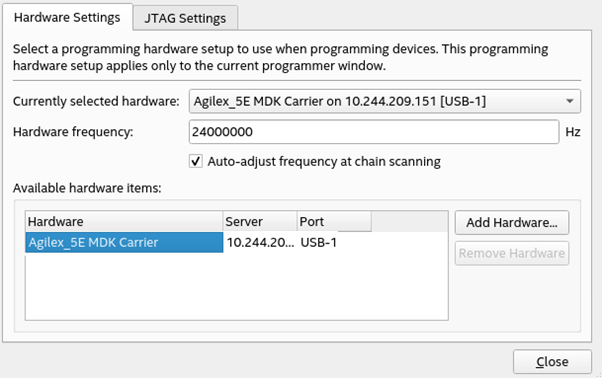
- For Currently selected hardware, select the Agilex™ 5 FPGA E-Series 065B Modular Development Kit and then click Close.
- Click Auto Detect to detect the JTAG device chain.
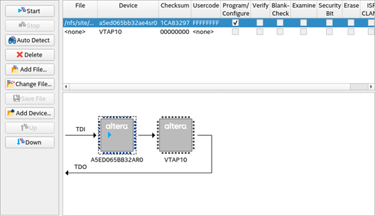
- Select the target FPGA device in the JTAG chain, click Change File, and select the FPGA configuration file pcie_ed.sof. Then, click Open.
- Check the Program/Configure option and click Start to start the FPGA configuration.
- Perform a warm reboot for the host system once the Agilex™ 5 FPGA is successfully configured.
- Check the enumeration of the PCIe Endpoint device ( Agilex™ 5 FPGA E-Series 065B Modular Development Kit) on the host system by running the “lspci –d 1172:” command in a Linux Terminal.
Expected result:
BDF Unassigned class [ff00]: Altera Corporation Device 0000 (rev 01)