A newer version of this document is available. Customers should click here to go to the newest version.
1. Overview
2. Quick Start Guide
3. Configuring and Generating the GTS AXI Multichannel DMA IP for PCI Express
4. Integrating the IP With Your Application
5. Simulating the IP
6. Validating the IP
A. Appendix A: Functional Description
B. Appendix B: Registers
C. Document Revision History for the GTS AXI Multichannel DMA IP for PCI Express*
2.1.1. Downloading and Installing Quartus® Prime Software
2.1.2. Configuring and Generating the GTS AXI Multichannel DMA IP for PCI Express
2.1.3. Configuring and Generating the GTS AXI Streaming Intel FPGA IP for PCI Express
2.1.4. Configuring and Generating the GTS System PLL Clocks Intel FPGA IP
2.1.5. Configuring and Generating the GTS Reset Sequencer Intel FPGA IP
2.1.6. Configuring and Generating the Reset Release IP
2.1.7. Instantiating and Connecting the IP Interfaces
2.1.8. Simulate, Compile and Validate the Design on Hardware
4.4.1. PCIe AXI-Stream TX Interface (ss_tx_st)
4.4.2. PCIe AXI-Stream RX Interface (ss_rx_st)
4.4.3. Control and Status Register Interface (ss_csr_lite)
4.4.4. Transmit Flow Control Credit Interface (ss_txcrdt)
4.4.5. Configuration Intercept Interface (CII)
4.4.6. Completion Timeout Interface (ss_cplto)
4.4.7. Function Level Reset (FLR) Interface
4.4.8. Control Shadow Interface (ss_ctrlshadow)
4.4.9. Error Interface
4.5.1. H2D AXI-Stream Manager (h2d_st_initatr)
4.5.2. D2H AXI-Stream Subordinate (d2h_st_respndr)
4.5.3. H2D/D2H AXI-MM Manager (dma_mm_initatr)
4.5.4. BAM AXI-MM Manager (bam_mm_initatr)
4.5.5. BAS AXI-MM Subordinate (bas_mm_respndr)
4.5.6. PIO AXI-Lite Manager (pio_lite_initiatr)
4.5.7. HIP Reconfiguration AXI-Lite Subordinate (user_csr_lite)
4.5.8. User Event MSI-X (user_msix)
4.5.9. User Event MSI (user_msi)
4.5.10. User Function Level Reset (user_flr)
4.5.11. User Configuration Intercept Interface
4.5.12. Configuration Slave (cs_lite_respndr)
A.1.1.1. H2D Data Mover
A.1.1.2. D2H Data Mover
A.1.1.3. Descriptors
A.1.1.4. AXI4-Lite PIO Manager
A.1.1.5. AXI-MM Write (H2D) and Read (D2H) Manager
A.1.1.6. AXI-Stream Manager (H2D) and Subordinate (D2H)
A.1.1.7. User MSI-X
A.1.1.8. User Function Level Reset (FLR)
A.1.1.9. Control and Status Registers
3.2.2.2.2.2. PCIe VF MSI-X
The VF MSI-X capability is available in Multichannel DMA, BAM+MCDMA and BAM+BAS+MCDMA user modes if the SR-IOV support is enabled and total VFs are non-zero.
Figure 19. PCIe VF MSI-X Parameters
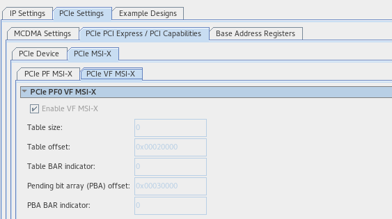
| Parameter | Value | Default Value | Description |
|---|---|---|---|
| Enable MSI-X | On / Off | See Description | Enables or disables the MSI-X capability.
Note: In Multichannel DMA, BAM+MCDMA and BAM+BAS+MCDMA user modes, the MSI-X capability is automatically enabled, and the capability registers are set by the IP Parameter Editor. You cannot modify the capability register values.
|
| Table Size | 0 - 1023 | 0 | Sets the number of entries in the MSI-X table. System software reads this field to determine the MSI-X table size N, which is encoded as N-1. |
| Table Offset | 0x00020000 | 0x00020000 | Sets the read-only base address of the MSI-X table. Points to the base of the MSI-X table. The lower 3 bits of the table BAR indicator (BIR) are set to zero by software to form a 64-bit qword-aligned offset. |
| Table BAR Indicator | 0 | 0 | Specifies which one of a function's base address registers, located beginning at 0x10 in the Configuration Space, maps the MSI-X table into memory space. |
| Pending Bit Array (PBA) Offset | 0x00030000 | 0x00030000 | Used as an offset from the address contained in one of the function's Base Address registers to point to the base of the MSI-X PBA. The lower 3 bits of the PBA BIR are set to zero by software to form a 32-bit qword-aligned offset. This field is read-only after being programmed. |
| PBA BAR Indicator | 0 | 0 | Specifies the function Base Address register, located beginning at 0x10 in Configuration Space, that maps the MSI-X PBA into memory space. This field is read-only in the MSI-X Capability Structure. |