Agilex® 7 FPGA F-Series Transceiver-SoC Development Kit User Guide
4.3. Control Onboard Clock through Clock Controller GUI
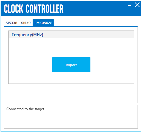
- Connect J51.2 to J26.19, J51.1 to J26.17 by duban wires, connect J26.12 to J26.11 by jumper. This set LMK05028 work at I2C mode and put it into I 2 C chain. Ensure SW10.2 is set to ON and SW4.4 is set to OFF.
- Generate the register file by using TICS Pro tools and MATLAB Runtime v9.0 (2015b, 64-bit).
- Import generated register file into on-board chip through Clock Controller GUI.
The instructions to run the Clock Controller GUI are stated in the Running the BTS GUI section. Alternatively, you can start using the Clock Controller feature by selecting the Clock icon on the BTS GUI.
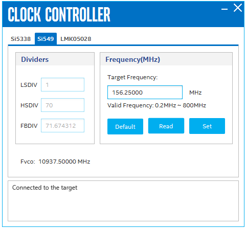
- LSDIV: Low Speed Output Divider
- HSDIV: High Speed Output Divider
- FBDIV: DSPLL* Feedback Divider used to set Digital VCO Frequency
The following sections describe the Clock Controller GUI buttons.
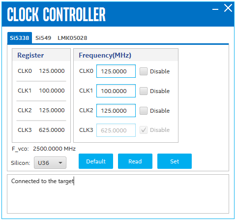
Read
Reads the current frequency setting for the oscillator associated with the active tab.
Default
Sets the frequency for the oscillator associated with the active tab back to its default value. You can also return to the default frequencies by power cycling the board.
Set
Sets the programmable oscillator frequency for the selected clock to the value in the CLKx output controls for the Si5338. Frequency changes might take several milliseconds to take effect. You might see glitches on the clock during this time. Altera recommends resetting the FPGA logic after changing frequencies.
Import