Video and Vision Processing Suite Intel® FPGA IP User Guide
ID
683329
Date
12/12/2022
Public
A newer version of this document is available. Customers should click here to go to the newest version.
1. About the Video and Vision Processing Suite
2. Getting Started with the Video and Vision Processing IPs
3. Video and Vision Processing IPs Functional Description
4. Video and Vision Processing IP Interfaces
5. Video and Vision Processing IP Registers
6. Video and Vision Processing IPs Software Programming Model
7. Protocol Converter Intel® FPGA IP
8. 3D LUT Intel® FPGA IP
9. AXI-Stream Broadcaster Intel® FPGA IP
10. Chroma Key Intel® FPGA IP
11. Chroma Resampler Intel® FPGA IP
12. Clipper Intel® FPGA IP
13. Clocked Video Input Intel® FPGA IP
14. Clocked Video to Full-Raster Converter Intel® FPGA IP
15. Clocked Video Output Intel® FPGA IP
16. Color Space Converter Intel® FPGA IP
17. Deinterlacer Intel® FPGA IP
18. FIR Filter Intel® FPGA IP
19. Frame Cleaner Intel® FPGA IP
20. Full-Raster to Clocked Video Converter Intel® FPGA IP
21. Full-Raster to Streaming Converter Intel® FPGA IP
22. Genlock Controller Intel® FPGA IP
23. Generic Crosspoint Intel® FPGA IP
24. Genlock Signal Router Intel® FPGA IP
25. Guard Bands Intel® FPGA IP
26. Interlacer Intel® FPGA IP
27. Mixer Intel® FPGA IP
28. Pixels in Parallel Converter Intel® FPGA IP
29. Scaler Intel® FPGA IP
30. Stream Cleaner Intel® FPGA IP
31. Switch Intel® FPGA IP
32. Tone Mapping Operator Intel® FPGA IP
33. Test Pattern Generator Intel® FPGA IP
34. Video Frame Buffer Intel® FPGA IP
35. Video Streaming FIFO Intel® FPGA IP
36. Video Timing Generator Intel® FPGA IP
37. Warp Intel® FPGA IP
38. Design Security
39. Document Revision History for Video and Vision Processing Suite User Guide
22.4.1. Achieving Genlock Controller Free Running (for Initialization or from Lock to Reference Clock N)
22.4.2. Locking to Reference Clock N (from Genlock Controller IP free running)
22.4.3. Setting the VCXO hold over
22.4.4. Restarting the Genlock Controller IP
22.4.5. Locking to Reference Clock N New (from Locking to Reference Clock N Old)
22.4.6. Changing to Reference Clock or VCXO Base Frequencies (switch between p50 and p59.94 video formats and vice-versa)
22.4.7. Disturbing a Reference Clock (a cable pull)
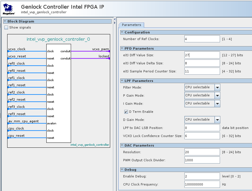
22.2. Genlock Controller IP Parameters
The IP offers compile- and run-time parameters
| Parameter | Values | Description |
|---|---|---|
| Configuration | ||
| Number of reference clock | 1 to 4 | The number of reference clocks as source for VCXO tracking. |
| PFD Parameters | ||
| Differential value size | 12 to 27 | The size of the PFD clock counters and output difference value.. |
| Differential value size | 8 to 24 | The number of bits for the error counter to calculate the difference between two samples of output difference values. |
| Sample period counter size | 4 to 32 | Select how many least significant bits (LSB) the IP uses for the sample period counter. |
| LPF Parameters | ||
| Filter Mode | Frequency Mode Phase Mode CPU selectable |
Select the filter mode |
| P Gain Mode | Positive Only Negative Only CPU selectable |
Select the proportional gain modes |
| I Gain Mode | Positive Only Negative Only CPU selectable |
Select the integral gain modes |
| D Term enable | On or off | Turn on the derivative term logic |
| D Gain Mode | Positive Only Negative Only CPU selectable |
Select the derivative gain modes. |
| LPF to DAC LSB Position | 0 to 3 | Select the LPF output to DAC least significant bit position. Allows the IP to ignore error wobble by moving the LSB. |
| VCXO Lock Confidence Counter Size | 6 to 32 | The lock confidence count size in bits. The number of successive samples with no error before the IP indicates lock. |
| DAC Parameters | ||
| Resolution | 8 to 24 | PWM DAC value output size. Defines the precision of the value to drive the DAC. Higher number of bits indicates more resolution, and longer time to lock. Fewer bits could decrease the locking time but increase the VCXO jitter. |
| PMW Output Clock Divider | 3 to 4096 | The IP divides the VCXO clock by this value (and then by an additional 2). The IP uses the value to drive the DAC output pin. The value should be low enough to provide a fast response, but not too low to increase VCXO jitter. |
| Debug | ||
| Enable Debug | 0 to 2 | Extra CPU debugging registers:
|
| CPU Clock Frequency | 1 MHz to 1 GHz | CPU clock frequency for measuring VCXO and reference clock frequencies for debugging, |
Figure 56. Genlock Controller IP Parameters