AN 584: Timing Closure Methodology for Advanced FPGA Designs
1.6.1. Excessive Logic Levels
Excessive levels of combinational logic in your design can increase the delay on a path and cause that path to become critical. The number of logic levels between registers may be difficult to visualize in your RTL code alone.
As an example, conditional statements are always translated as additional levels of logic. Verify situations before adding conditional statements within another conditional statement. Ensure that the modifications you make apply the conditions only on the branch where it is necessary.
The example below shows a section of a Verilog HDL code. Assume that counter1 is an 8-bit counter, and that counter2 is a 12-bit counter. TC1 and TC2 represent the status count signals for these counters:
if (reset == 0) begin
   counter1 <= 0;
   counter2 <= 0;
   TC1 <= 1'b0;
   TC2 <= 1'b0;

   end else begin
   if (incr ==1) begin
      if (counter1 == value1) begin
         TC1 <= 1'b1;
         if (counter2 == value2) begin
            TC2 <= 1'b1 ;
         end else begin
            counter2 <= counter2 +1 ;
         end
      end else begin
         counter1 <= counter1 +1 ;
   end

end
The updates for counter2 are based on the results of the nested 8-bit and 12-bit comparators. Depending on the device architecture, this combinational logic that implements in several levels can form a critical path. The way the logic maps can affect the number of constituent delays.
The Timing Analyzer design metric reports provide a summary of the logic depths in your design per clock domain.
In the Timing Analyzer, click Tasks > Reports > Design Metrics > Report Logic Depth to generate this report.
Figure 5 shows clk_2x domain’s worst depth is at 4. You can check the paths with this depth by right-clicking on the clock domain and depth element to generate a timing report.
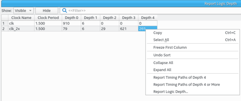
The report indicates that the path with the longest depth belongs to the nested comparators in the example, and is contributing to several critical paths on the design.
The Data Path tab report on the right shows all the interconnected elements, while the Statistics tab report on the left shows a summary of the total cells and interconnect delays (IC). In this case, the delay contributes the biggest percentage on the total delay of the data path at 41% and 45% respectively.
To correct this condition, it is possible to check the required conditions in parallel with, or before the results are available from other logical operations. By doing so, you can reduce the delay on the critical path.
In some cases, it may not be possible to modify the logic by parallel operations. In these cases, you can consider using pipeline registers to split the logic operations that occur in one cycle. You must account for the effect of this added latency in other parts of the design if you use this approach.
Perform the following general guidelines to fix failing critical register-to-register paths:
- Give priority to improving the code instead of modifying the Compiler Settings.
- Analyze whether critical paths can be re-coded.
- Check if logic can be pushed across register boundaries.
- Check if part of the logic can be done in parallel, or in a different data cycle (a cycle before or later).
- When you modify code, be aware of the implementation in hardware.
- If you are working on a block within a larger design, target a higher than required timing performance prior to block integration.