Embedded Peripherals IP User Guide

ID 683130
Date 8/11/2025
Public
Document Table of Contents
1. Introduction 2. Avalon® -ST Single-Clock and Dual-Clock FIFO Cores 3. Avalon® -ST Serial Peripheral Interface Core 4. SPI Core 5. SPI Agent/JTAG to Avalon® Host Bridge Cores 6. Intel eSPI Agent Core 7. eSPI to LPC Bridge Core 8. Ethernet MDIO Core 9. Intel FPGA 16550 Compatible UART Core 10. UART Core 11. JTAG UART Core 12. Intel FPGA Avalon® Mailbox Core 13. Intel FPGA Avalon® Mutex Core 14. Intel FPGA Avalon® I2C (Host) Core 15. Intel FPGA I2C Agent to Avalon® -MM Host Bridge Core 16. Intel FPGA Avalon® Compact Flash Core 17. EPCS/EPCQA Serial Flash Controller Core 18. Intel FPGA Serial Flash Controller Core 19. Intel FPGA Serial Flash Controller II Core 20. Intel FPGA Generic QUAD SPI Controller Core 21. Intel FPGA Generic QUAD SPI Controller II Core 22. Interval Timer Core 23. Intel FPGA Avalon FIFO Memory Core 24. On-Chip Memory (RAM and ROM) Intel FPGA IP 25. On-Chip Memory II (RAM or ROM) Intel FPGA IP 26. Optrex 16207 LCD Controller Core 27. PIO Core 28. PLL Cores 29. DMA Controller Core 30. Modular Scatter-Gather DMA Core 31. Scatter-Gather DMA Controller Core 32. SDRAM Controller Core 33. Tri-State SDRAM Core 34. Video Sync Generator and Pixel Converter Cores 35. Intel FPGA Interrupt Latency Counter Core 36. Performance Counter Unit Core 37. Vectored Interrupt Controller Core 38. Avalon® -ST Data Pattern Generator and Checker Cores 39. Avalon® -ST Test Pattern Generator and Checker Cores 40. System ID Peripheral Core 41. Avalon® Packets to Transactions Converter Core 42. Avalon® -ST Multiplexer and Demultiplexer Cores 43. Avalon® -ST Bytes to Packets and Packets to Bytes Converter IP 44. Avalon® -ST Delay Core 45. Avalon® -ST Round Robin Scheduler Core 46. Avalon® -ST Splitter Core 47. Avalon® -MM DDR Memory Half Rate Bridge Core 48. Intel FPGA GMII to RGMII Converter Core 49. HPS GMII to RGMII Adapter Intel® FPGA IP 50. Intel FPGA MII to RMII Converter Core 51. HPS GMII to TSE 1000BASE-X/SGMII PCS Bridge Core Intel® FPGA IP 52. Intel FPGA HPS EMAC to Multi-rate PHY GMII Adapter Core 53. Intel FPGA MSI to GIC Generator Core 54. Cache Coherency Translator Intel® FPGA IP 55. Altera ACE5-Lite Cache Coherency Translator 56. Lightweight UART Core

15.2.5. Write Operation

The Avalon® write data width is 32 bits wide. A 32-bit width limits the bridge to only issue word align Avalon® addresses. It also allows the upstream I2C host to write to any sequence of bytes on any address alignment. There is a conversion logic which sits between the Avalon® interface and the I2C interface.

Write operation conversion logic flow:

  • Checks the address alignment issued by the I2C host.
  • Enables data by setting byteenable high to indicate which byte address the I2C host wants to write into.
    Note: If the address issued by I2C host is 0x03h, the byteenable is 4’b1000.
  • Combines multiple bytes of data into a 32-bit packet if their addresses are sequential.
    Note: If the first write is to address 0x04 and the second write is to address 0x05, then byteenable is 4’b0011.

Legal byteenable combinations are 4’b0001, 4’b0010, 4’b0100, 4’b1000, 4’b0011, 4’b1100 and 4’b1111.

  • If the write request issued by the I2C host ends up with an illegal byteenable combination such as, 4’b0110, 4’b0111, or 4’b1110, then the bridge generates multiple Avalon® byte writes.
    Note: If the sequential write request from the I2C host starts from 0x0 and ends at 0x02 (illegal byteenable, b’0111), then the bridge will generate three Avalon® write requests with legal byteenable 4’b0001, 4’b0010 and 4’b0100.
  • Issues a word align Avalon® address according to the address sent by the I2C host with the two LSB set to zero.

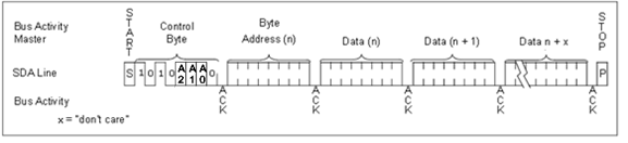
Upon receiving of the agent address with the R/W bit set to zero, the bridge issues an acknowledge to the I2C host. The next byte transmitted by the host is the byte address. The byte address is written into the address counter inside the bridge. The bridge acknowledges the I2C host again and the host transmits the data byte to be written into the addressed memory location. The host keeps sending data bytes to the bridge and terminates the operation with a Stop condition at the end.

Figure 59. Write Operation