A newer version of this document is available. Customers should click here to go to the newest version.
1. FPGA AI Suite Design Examples User Guide
2. FPGA AI Suite Design Examples
3. [PCIE] Getting Started with the FPGA AI Suite PCIe* -based Design Example
4. [PCIE] Building the FPGA AI Suite Runtime
5. [PCIE] Running the Design Example Demonstration Applications
6. [PCIE] Design Example Components
7. [PCIE] Design Example System Architecture for the Agilex™ 7 FPGA
8. [OFS-PCIE] Getting Started with Open FPGA Stack (OFS) for PCIe* Attach Design Examples
9. [OFS-PCIE] Design Example Components
10. [HL-NO-DDR] Getting Started with the FPGA AI Suite DDR-Free Design Example
11. [HL-NO-DDR] Running the Hostless DDR-Free Design Example
12. [HL-NO-DDR] Design Example System Architecture
13. [HL-NO-DDR] Quartus® Prime System Console
14. [HL-NO-DDR] JTAG to Avalon MM Host Register Map
15. [HL-NO-DDR] Updating MIF Files
16. [HL-JTAG] Getting Started
17. [HL-JTAG] Design Example Components
18. [SOC] FPGA AI Suite SoC Design Example Prerequisites
19. [SOC] FPGA AI Suite SoC Design Example Quick Start Tutorial
20. [SOC] FPGA AI Suite SoC Design Example Run Process
21. [SOC] FPGA AI Suite SoC Design Example Build Process
22. [SOC] FPGA AI Suite SoC Design Example Quartus® Prime System Architecture
23. [SOC] FPGA AI Suite SoC Design Example Software Components
24. [SOC] Streaming-to-Memory (S2M) Streaming Demonstration
A. FPGA AI Suite Example Designs User Guide Archives
B. FPGA AI Suite Example Designs User Guide Revision History
5.1. [PCIE] Exporting Trained Graphs from Source Frameworks
5.2. [PCIE] Compiling Exported Graphs Through the FPGA AI Suite
5.3. [PCIE] Compiling the PCIe* -based Example Design
5.4. [PCIE] Programming the FPGA Device ( Agilex™ 7)
5.5. [PCIE] Performing Accelerated Inference with the dla_benchmark Application
5.6. [PCIE] Running the Ported OpenVINO™ Demonstration Applications
8.2.1. [OFS-PCIE] Setup the OFS Environment for the FPGA Device
8.2.2. [OFS-PCIE] Exporting Trained Graphs from Source Frameworks.
8.2.3. [OFS-PCIE] Compiling Exported Graphs Through the FPGA AI Suite
8.2.4. [OFS-PCIE] Compiling the OFS for PCIe* Attach Design Example
8.2.5. [OFS-PCIE] Programming the FPGA Green Bitstream
8.2.6. [OFS-PCIE] Performing Accelerated Inference with the dla_benchmark application
16.1. [HL-JTAG] Prerequisites
16.2. [HL-JTAG] Building the FPGA AI Suite Runtime
16.3. [HL-JTAG] Building an FPGA Bitstream for the JTAG Design Examples
16.4. [HL-JTAG] Programming the FPGA Device
16.5. [HL-JTAG] Preparing Graphs for Inference with FPGA AI Suite
16.6. [HL-JTAG] Performing Inference on the Agilex™ 5 FPGA E-Series 065B Premium Development Kit
16.7. [HL-JTAG] Inference Performance Measurement
16.8. [HL-JTAG] Known Issues and Limitations
19.1. [SOC] Initial Setup
19.2. [SOC] Initializing a Work Directory
19.3. [SOC] (Optional) Create an SD Card Image (.wic)
19.4. [SOC] Writing the SD Card Image (.wic) to an SD Card
19.5. [SOC] Preparing SoC FPGA Development Kits for the FPGA AI Suite SoC Design Example
19.6. [SOC] Adding Compiled Graphs (AOT files) to the SD Card
19.7. [SOC] Verifying FPGA Device Drivers
19.8. [SOC] Running the Demonstration Applications
19.5.1. [SOC] Preparing the Agilex™ 7 FPGA I-Series Transceiver-SoC Development Kit
19.5.2. [SOC] Preparing the Arria® 10 SX SoC FPGA Development Kit (DK-SOC-10AS066S)
19.5.3. [SOC] Configuring the SoC FPGA Development Kit UART Connection
19.5.4. [SOC] Determining the SoC FPGA Development Kit IP Address
19.5.1.1. [SOC] Confirming Agilex™ 7 FPGA I-Series Transceiver-SoC Development Kit Board Set Up
19.5.1.2. [SOC] Programming the Agilex™ 7FPGA Device with the JTAG Indirect Configuration (.jic) File
19.5.1.3. [SOC] Connecting the Agilex™ 7 FPGA I-Series Transceiver-SoC Development Kit to the Host Development System
22.1. [SOC] FPGA AI Suite SoC Design Example Inference Sequence Overview
22.2. [SOC] Memory-to-Memory (M2M) Variant Design
22.3. [SOC] Streaming-to-Memory (S2M) Variant Design
22.4. [SOC] Top Level
22.5. [SOC] The SoC Design Example Platform Designer System
22.6. [SOC] Fabric EMIF Design Component
22.7. [SOC] PLL Configuration
23.1.1. [SOC] Yocto Recipe: recipes-core/images/coredla-image.bb
23.1.2. [SOC] Yocto Recipe: recipes-bsp/u-boot/u-boot-socfpga_%.bbappend
23.1.3. [SOC] Yocto Recipe: recipes-drivers/msgdma-userio/msgdma-userio.bb
23.1.4. [SOC] Yocto Recipe: recipes-drivers/uio-devices/uio-devices.bb
23.1.5. [SOC] Yocto Recipe: recipes-kernel/linux/linux-socfpga-lts_%.bbappend
23.1.6. [SOC] Yocto Recipe: recipes-support/devmem2/devmem2_2.0.bb
23.1.7. [SOC] Yocto Recipe: wic
22.4. [SOC] Top Level
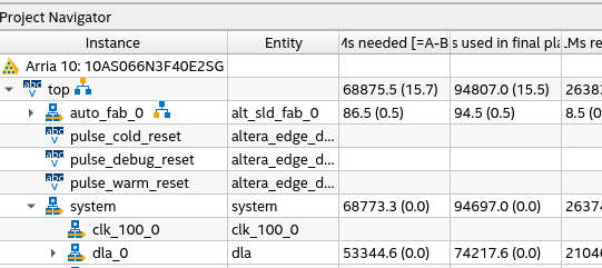
After the Quartus® Prime project has finished compiling, the design should look similar to the following image in the Quartus® Prime Project Navigator:
Figure 20. SoC Design Example Hierarchy
The top-level Verilog file and HPS configuration is derived directly from the GSRD designs located at RocketBoards.org:
- For more information about the GSRD for the Agilex™ 7 FPGA I-Series Transceiver-SoC Development Kit, refer to the following URL https://www.rocketboards.org/foswiki/Documentation/AgilexSoCGSRDSIAGI027
- For more information about the GSRD for the Arria® 10 SX SoC FPGA Development Kit (DK-SOC-10AS066S), refer to the following URL: https://www.rocketboards.org/foswiki/Documentation/arria10SoCGSRD
The GSRD designs have been modified to include the FPGA AI Suite IP. All unnecessary logic has been removed, which provides a concise design example.
The main FPGA AI Suite SoC design example is contained within a single Platform Designer system, called system. Double-click this node in the Quartus® Prime Project Navigator to launch Platform Designer.