A newer version of this document is available. Customers should click here to go to the newest version.
1. FPGA AI Suite Design Examples User Guide
2. FPGA AI Suite Design Examples
3. [PCIE] Getting Started with the FPGA AI Suite PCIe* -based Design Example
4. [PCIE] Building the FPGA AI Suite Runtime
5. [PCIE] Running the Design Example Demonstration Applications
6. [PCIE] Design Example Components
7. [PCIE] Design Example System Architecture for the Agilex™ 7 FPGA
8. [OFS-PCIE] Getting Started with Open FPGA Stack (OFS) for PCIe* Attach Design Examples
9. [OFS-PCIE] Design Example Components
10. [HL-NO-DDR] Getting Started with the FPGA AI Suite DDR-Free Design Example
11. [HL-NO-DDR] Running the Hostless DDR-Free Design Example
12. [HL-NO-DDR] Design Example System Architecture
13. [HL-NO-DDR] Quartus® Prime System Console
14. [HL-NO-DDR] JTAG to Avalon MM Host Register Map
15. [HL-NO-DDR] Updating MIF Files
16. [HL-JTAG] Getting Started
17. [HL-JTAG] Design Example Components
18. [SOC] FPGA AI Suite SoC Design Example Prerequisites
19. [SOC] FPGA AI Suite SoC Design Example Quick Start Tutorial
20. [SOC] FPGA AI Suite SoC Design Example Run Process
21. [SOC] FPGA AI Suite SoC Design Example Build Process
22. [SOC] FPGA AI Suite SoC Design Example Quartus® Prime System Architecture
23. [SOC] FPGA AI Suite SoC Design Example Software Components
24. [SOC] Streaming-to-Memory (S2M) Streaming Demonstration
A. FPGA AI Suite Example Designs User Guide Archives
B. FPGA AI Suite Example Designs User Guide Revision History
5.1. [PCIE] Exporting Trained Graphs from Source Frameworks
5.2. [PCIE] Compiling Exported Graphs Through the FPGA AI Suite
5.3. [PCIE] Compiling the PCIe* -based Example Design
5.4. [PCIE] Programming the FPGA Device ( Agilex™ 7)
5.5. [PCIE] Performing Accelerated Inference with the dla_benchmark Application
5.6. [PCIE] Running the Ported OpenVINO™ Demonstration Applications
8.2.1. [OFS-PCIE] Setup the OFS Environment for the FPGA Device
8.2.2. [OFS-PCIE] Exporting Trained Graphs from Source Frameworks.
8.2.3. [OFS-PCIE] Compiling Exported Graphs Through the FPGA AI Suite
8.2.4. [OFS-PCIE] Compiling the OFS for PCIe* Attach Design Example
8.2.5. [OFS-PCIE] Programming the FPGA Green Bitstream
8.2.6. [OFS-PCIE] Performing Accelerated Inference with the dla_benchmark application
16.1. [HL-JTAG] Prerequisites
16.2. [HL-JTAG] Building the FPGA AI Suite Runtime
16.3. [HL-JTAG] Building an FPGA Bitstream for the JTAG Design Examples
16.4. [HL-JTAG] Programming the FPGA Device
16.5. [HL-JTAG] Preparing Graphs for Inference with FPGA AI Suite
16.6. [HL-JTAG] Performing Inference on the Agilex™ 5 FPGA E-Series 065B Premium Development Kit
16.7. [HL-JTAG] Inference Performance Measurement
16.8. [HL-JTAG] Known Issues and Limitations
19.1. [SOC] Initial Setup
19.2. [SOC] Initializing a Work Directory
19.3. [SOC] (Optional) Create an SD Card Image (.wic)
19.4. [SOC] Writing the SD Card Image (.wic) to an SD Card
19.5. [SOC] Preparing SoC FPGA Development Kits for the FPGA AI Suite SoC Design Example
19.6. [SOC] Adding Compiled Graphs (AOT files) to the SD Card
19.7. [SOC] Verifying FPGA Device Drivers
19.8. [SOC] Running the Demonstration Applications
19.5.1. [SOC] Preparing the Agilex™ 7 FPGA I-Series Transceiver-SoC Development Kit
19.5.2. [SOC] Preparing the Arria® 10 SX SoC FPGA Development Kit (DK-SOC-10AS066S)
19.5.3. [SOC] Configuring the SoC FPGA Development Kit UART Connection
19.5.4. [SOC] Determining the SoC FPGA Development Kit IP Address
19.5.1.1. [SOC] Confirming Agilex™ 7 FPGA I-Series Transceiver-SoC Development Kit Board Set Up
19.5.1.2. [SOC] Programming the Agilex™ 7FPGA Device with the JTAG Indirect Configuration (.jic) File
19.5.1.3. [SOC] Connecting the Agilex™ 7 FPGA I-Series Transceiver-SoC Development Kit to the Host Development System
22.1. [SOC] FPGA AI Suite SoC Design Example Inference Sequence Overview
22.2. [SOC] Memory-to-Memory (M2M) Variant Design
22.3. [SOC] Streaming-to-Memory (S2M) Variant Design
22.4. [SOC] Top Level
22.5. [SOC] The SoC Design Example Platform Designer System
22.6. [SOC] Fabric EMIF Design Component
22.7. [SOC] PLL Configuration
23.1.1. [SOC] Yocto Recipe: recipes-core/images/coredla-image.bb
23.1.2. [SOC] Yocto Recipe: recipes-bsp/u-boot/u-boot-socfpga_%.bbappend
23.1.3. [SOC] Yocto Recipe: recipes-drivers/msgdma-userio/msgdma-userio.bb
23.1.4. [SOC] Yocto Recipe: recipes-drivers/uio-devices/uio-devices.bb
23.1.5. [SOC] Yocto Recipe: recipes-kernel/linux/linux-socfpga-lts_%.bbappend
23.1.6. [SOC] Yocto Recipe: recipes-support/devmem2/devmem2_2.0.bb
23.1.7. [SOC] Yocto Recipe: wic
19.5.1.1. [SOC] Confirming Agilex™ 7 FPGA I-Series Transceiver-SoC Development Kit Board Set Up
Confirm the board settings as follows:
- Ensure that the Agilex™ 7 FPGA I-Series Transceiver-SoC Development Kit has the required DIP switch and jumper settings. The SoC example design requires that all DIP switches have their default settings except for S9 where switch 1 is ON and switches 2,3, and 4 are OFF:
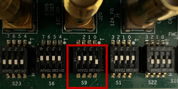
For more details about default DIP switch and jumper settings, refer to Agilex™ 7 FPGA I-Series Transceiver-SoC Development Kit User Guide .
- Ensure that the HPS IO48 OOBE daughter card is installed in connector J4 on the development kit, and the SD card with the programmed Yocto image is installed in the daughter card.
- Ensure that the DDR4 x8 RDIMM is installed in the PCIe slot furthest from the fan. For RDIMM requirements, refer to [SOC] Agilex 7 FPGA I-Series Transceiver-SoC Development Kit Hardware Requirements.
When configured and connected, the Agilex™ 7 FPGA I-Series Transceiver-SoC Development Kit should resemble the following image:
The board connections serve the following purposes:
-
The USB 2.0 connector is used to program the FPGA device.
-
The Ethernet connector is used for fast data transfer to the HPS.
-
The micro USB connector is used to monitor the serial output from, and provide command-line input to the HPS during operation.