Multi Channel DMA for PCI Express* Intel® FPGA IP Design Example User Guide
ID
683517
Date
2/06/2022
Public
A newer version of this document is available. Customers should click here to go to the newest version.
3.5.2.6.1. Build and Install Netdev Driver
3.5.2.6.2. Enable VFs if SRIOV is Supported
3.5.2.6.3. Configure the Number of Channels Supported on the Device
3.5.2.6.4. Configure the MTU Value
3.5.2.6.5. Configure the Device Communication
3.5.2.6.6. Configure Transmit Queue Selection Mechanism
3.5.2.6.7. Test Procedure by Using Name Space Environment
3.5.2.6.8. PIO Test
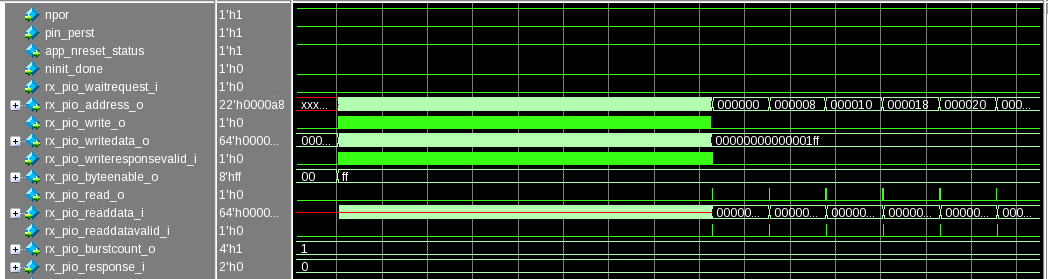
2.3.1.1.1. Simulation Result
Testbench writes 4 KB of incrementing pattern to on-chip memory and read back via Avalon-MM PIO interface. This design example testbench doesn’t simulate H2D/D2H data movers.
Figure 2. Simulation Log
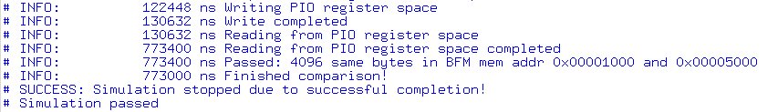
Figure 3. Simulation Waveform