Video and Vision Processing Suite Intel® FPGA IP User Guide
ID
683329
Date
6/26/2023
Public
A newer version of this document is available. Customers should click here to go to the newest version.
1. About the Video and Vision Processing Suite
2. Getting Started with the Video and Vision Processing IPs
3. Video and Vision Processing IPs Functional Description
4. Video and Vision Processing IP Interfaces
5. Video and Vision Processing IP Registers
6. Video and Vision Processing IPs Software Programming Model
7. Protocol Converter Intel® FPGA IP
8. 3D LUT Intel® FPGA IP
9. AXI-Stream Broadcaster Intel® FPGA IP
10. Bits per Color Sample Adapter Intel FPGA IP
11. Chroma Key Intel® FPGA IP
12. Chroma Resampler Intel® FPGA IP
13. Clipper Intel® FPGA IP
14. Clocked Video Input Intel® FPGA IP
15. Clocked Video to Full-Raster Converter Intel® FPGA IP
16. Clocked Video Output Intel® FPGA IP
17. Color Space Converter Intel® FPGA IP
18. Deinterlacer Intel® FPGA IP
19. FIR Filter Intel® FPGA IP
20. Frame Cleaner Intel® FPGA IP
21. Full-Raster to Clocked Video Converter Intel® FPGA IP
22. Full-Raster to Streaming Converter Intel® FPGA IP
23. Genlock Controller Intel® FPGA IP
24. Generic Crosspoint Intel® FPGA IP
25. Genlock Signal Router Intel® FPGA IP
26. Guard Bands Intel® FPGA IP
27. Interlacer Intel® FPGA IP
28. Mixer Intel® FPGA IP
29. Pixels in Parallel Converter Intel® FPGA IP
30. Scaler Intel® FPGA IP
31. Stream Cleaner Intel® FPGA IP
32. Switch Intel® FPGA IP
33. Tone Mapping Operator Intel® FPGA IP
34. Test Pattern Generator Intel® FPGA IP
35. Video and Vision Monitor Intel FPGA IP
36. Video Frame Buffer Intel® FPGA IP
37. Video Frame Reader Intel FPGA IP
38. Video Frame Writer Intel FPGA IP
39. Video Streaming FIFO Intel® FPGA IP
40. Video Timing Generator Intel® FPGA IP
41. Warp Intel® FPGA IP
42. Design Security
43. Document Revision History for Video and Vision Processing Suite User Guide
23.4.1. Achieving Genlock Controller Free Running (for Initialization or from Lock to Reference Clock N)
23.4.2. Locking to Reference Clock N (from Genlock Controller IP free running)
23.4.3. Setting the VCXO hold over
23.4.4. Restarting the Genlock Controller IP
23.4.5. Locking to Reference Clock N New (from Locking to Reference Clock N Old)
23.4.6. Changing to Reference Clock or VCXO Base Frequencies (switch between p50 and p59.94 video formats and vice-versa)
23.4.7. Disturbing a Reference Clock (a cable pull)
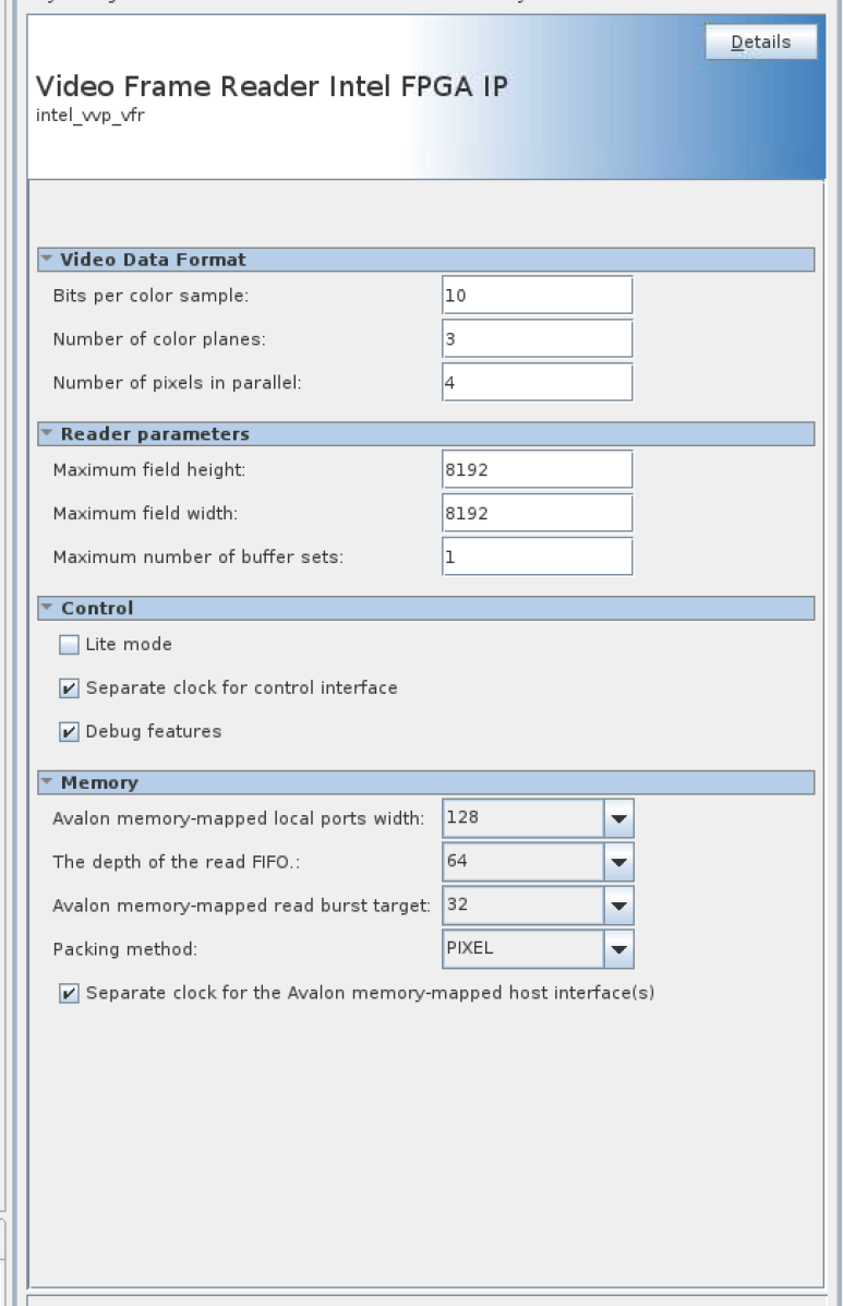
37.2. Video Frame Reader IP Parameters
The IP offers compile-time parameters.
| Parameter | Values | Description |
|---|---|---|
| Video Data Format | ||
| Bits per color sample | 8 to 16 | Select the number of bits per color sample. |
| Number of color planes | 1 to 4 | Select the number of color planes per pixel. |
| Number of pixels in parallel | 1 to 8 | Select the number of pixels in parallel. |
| Maximum Frame Size | ||
| Maximum frame height | 32 to 16384 | Select the maximum height of frames. If you attempt to read out fields or frames taller than this value, the IP crops them to this height. |
| Maximum frame width | 32 to 16384 | Select the maximum width of frames. If you attempt to read out fields or frames wider than this value, the IP crops them to this width. If you use the IP exclusively to read frames with 420 subsampling, optionally halve the maximum frame width entry in the GUI. Halving the entry optimizes memory footprint because of the more efficient 420 pixel packing. |
| Maximum number of buffer sets | 1 to 16 | Select the maximum number of buffer sets. Each buffer set implements a set of 16 additional control registers. To save resources configure the maximum number of buffer sets required for your application and no more. Most applications only require 1 or 2 buffer sets. |
| Control | ||
| Lite mode | On or off | Turn on to operate the frame reader in lite mode. |
Figure 83. Frame Reader IP GUI