1. Introduction to MAX® 10 FPGA B610 Package Thermal Design Guidelines
2. MAX® 10 FPGA B610 Package Mechanical Construction
3. MAX® 10 FPGA B610 Package CTM Construction
4. Quartus Requirements and Power Estimation
5. General FPGA Thermal Design Considerations
6. Thermal Design Process
7. Thermal Solution Mechanical Design
8. Vendor References
9. Document Revision History for the MAX® 10 FPGA B610 Package Thermal Design User Guide
A. Thermal Design Elements
2. MAX® 10 FPGA B610 Package Mechanical Construction
The MAX® 10 FPGA B610 package uses wire bond BGA package technology. The BGA die is mounted on the substrate and connected to the substrate by wire bonding technology.
The BGA package consists of an array of solder balls on the bottom of the package, which are used to connect the FPGA to the PCB. It is widely used for their high pin count and excellent thermal and electrical performance.
Figure 2. MAX® 10 FPGA B610 Package Mechanical Drawing
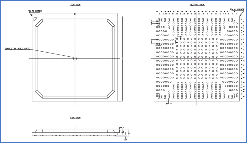
The package mechanical drawing provides a reference for PCB layout and design, to ensure proper alignment and soldering during assembly.
Each compact thermal model (CTM) is provided with the relevant package mechanical drawing (PMD). Contact your Altera FAE for more information.