AN 882: Using ADI AD9217 with Intel® Stratix® 10 Devices
ID
683700
Date
8/17/2020
Public
1.1. Hardware Requirements
1.2. Hardware Setup
1.3. Design Description
1.4. Functional Description
1.5. Parameterization
1.6. Directory Structure
1.7. Simulation
1.8. Latency Measurement for 10G Design
1.9. Register Map
1.10. Document Revision History for AN 882: Using ADI AD9217 with Intel Stratix 10 Devices
1.11. Appendix: 5G Design Example
1.11.5.1. Procedure
The scripts to run the commands are available in the Intel® Quartus® Prime Pro Edition software archive. The Intel® Quartus® Prime Pro Edition software archive should be extracted into the same folder.
- Ensure the device clock is available to the FPGA before proceeding to program the FPGA using SOF file.
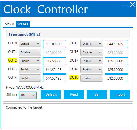
- The Intel® Stratix® 10 H-Tile Signal Integrity Development Kit has a Si5341 clock controller. Program 312.5 MHz in the Out_2 and Out_9 of Si5341 U6 silicon. Out_2 acts as device clock to the FPGA and Out_9 acts as the reference clock to the external clock source board.
Figure 24. Si5341 Clock Controller
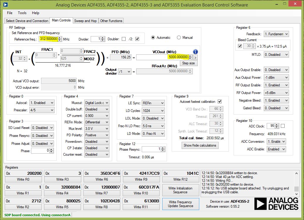
- After providing the device clock to the FPGA, program the FPGA using the SOF file. Then, provide 5000 MHz of sampling clock to the ADC through the external clock source board. In this case, ADF4355 is used as the external clock source board to generate sampling clock to the ADC.
Figure 25. ADF4355 External Clock Source
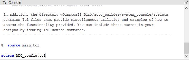
- After programming the clock source and SOF, in the Intel® Quartus® Prime Pro Edition software, select Tools > System Debugging Tools > System Console to launch the system console.
- In the Tcl console pane, type cd <full_path> to change directory to your project folder. If your project is already opened in the Intel® Quartus® Prime Pro Edition software, the default path of the system console is your project folder.
- All the examples shown are mainly for the mode where L is 16, lane rate is 5 Gbps, and ADC Sampling clock is 5000 MHz.
- Type the following commands in sequence and check the link up in the Signal Tap Logic Analyzer.
- source main.tcl
- source ADC_config.tcl
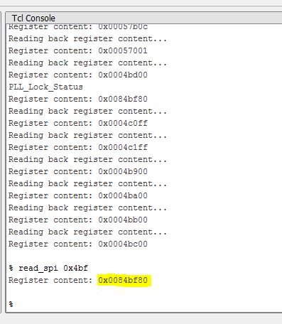
- After the successful link up, check the ADC PLL lock status by reading the register 0x04BF. It should be read as 0x80 if the link up is successful.
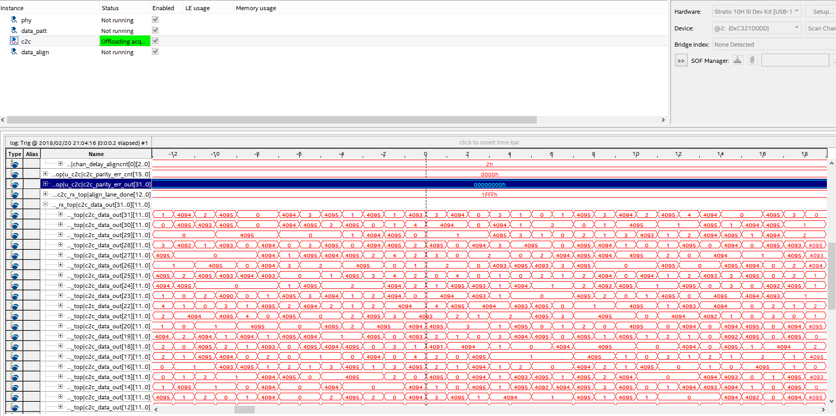
- Monitor the parity error output signal (c2c_parity_err_out) in the Signal Tap c2c instance for 0x000000h, if there is no parity error.
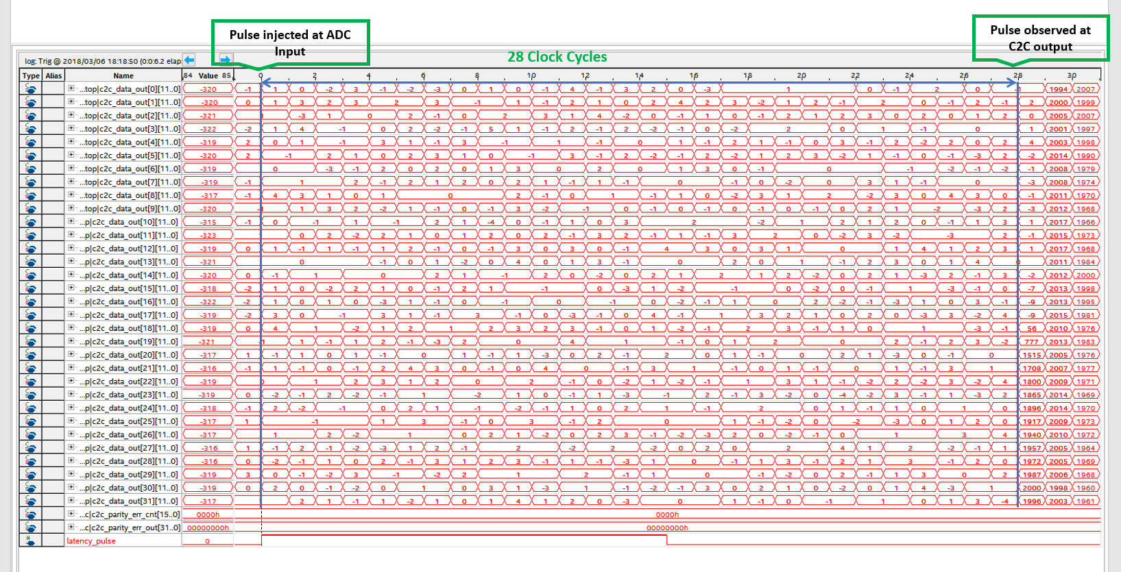
Figure 26. C2C Data Capture
- Calculate the latency measurement in the design by injecting a pulse to the ADC from the FPGA. The difference in clock counts between the pulse injected and the pulse observed at the C2C output gives the exact latency in the design. Refer Latency Measurement for 5G Design for the detailed description.
Figure 27. C2C Hardware Design Latency