AN 882: Using ADI AD9217 with Intel® Stratix® 10 Devices
ID
683700
Date
8/17/2020
Public
1.1. Hardware Requirements
1.2. Hardware Setup
1.3. Design Description
1.4. Functional Description
1.5. Parameterization
1.6. Directory Structure
1.7. Simulation
1.8. Latency Measurement for 10G Design
1.9. Register Map
1.10. Document Revision History for AN 882: Using ADI AD9217 with Intel Stratix 10 Devices
1.11. Appendix: 5G Design Example
1.11.6. Latency Measurement for 5G Design
The latency measurement in the low latency chip-to-chip (C2C) interface is performed based on the following specified sequences for 5G design:
- Latency pulse is generated in the FPGA (SMA J64) and it is fed as an input to the J2 VIN of the ADC AD9217 EVM board through the SMA cable.
Figure 28. Test Setup—Latency Measurement for 5G Design
 Figure 29. Block Diagram—Latency Measurement
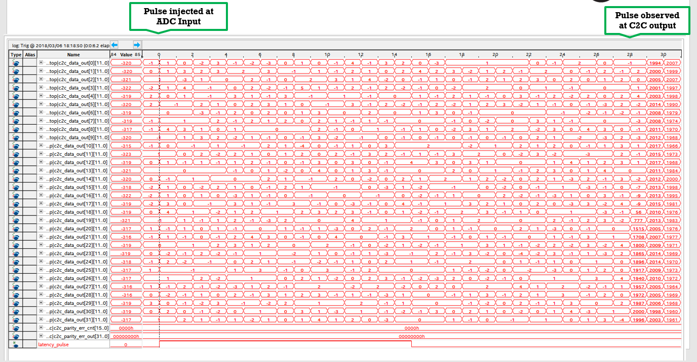
 - The pulse is injected at the input of ADC(AD9217) and is observed at the C2C output in the FPGA.
- The number of clock cycles between the pulse injected is observed at the C2C output, which is referred to as Chip-to-Chip latency.
- In Figure 30, the latency pulse is injected at the 0th clock cycle and the latency pulse in C2C data output is observed at the 28th clock cycle.
Figure 30. Latency Measurement for 5G Design