AN 882: Using ADI AD9217 with Intel® Stratix® 10 Devices
ID
683700
Date
8/17/2020
Public
1.1. Hardware Requirements
1.2. Hardware Setup
1.3. Design Description
1.4. Functional Description
1.5. Parameterization
1.6. Directory Structure
1.7. Simulation
1.8. Latency Measurement for 10G Design
1.9. Register Map
1.10. Document Revision History for AN 882: Using ADI AD9217 with Intel Stratix 10 Devices
1.11. Appendix: 5G Design Example
1.11.1. Hardware Setup
An Intel® Stratix® 10 GX H-Tile Signal Integrity Development Kit is used with the ADI AD9217 EVM attached to the FPGA Mezzanine Card Plus (FMC+) connector of the development board.
Figure 15. Hardware Setup—5G Design
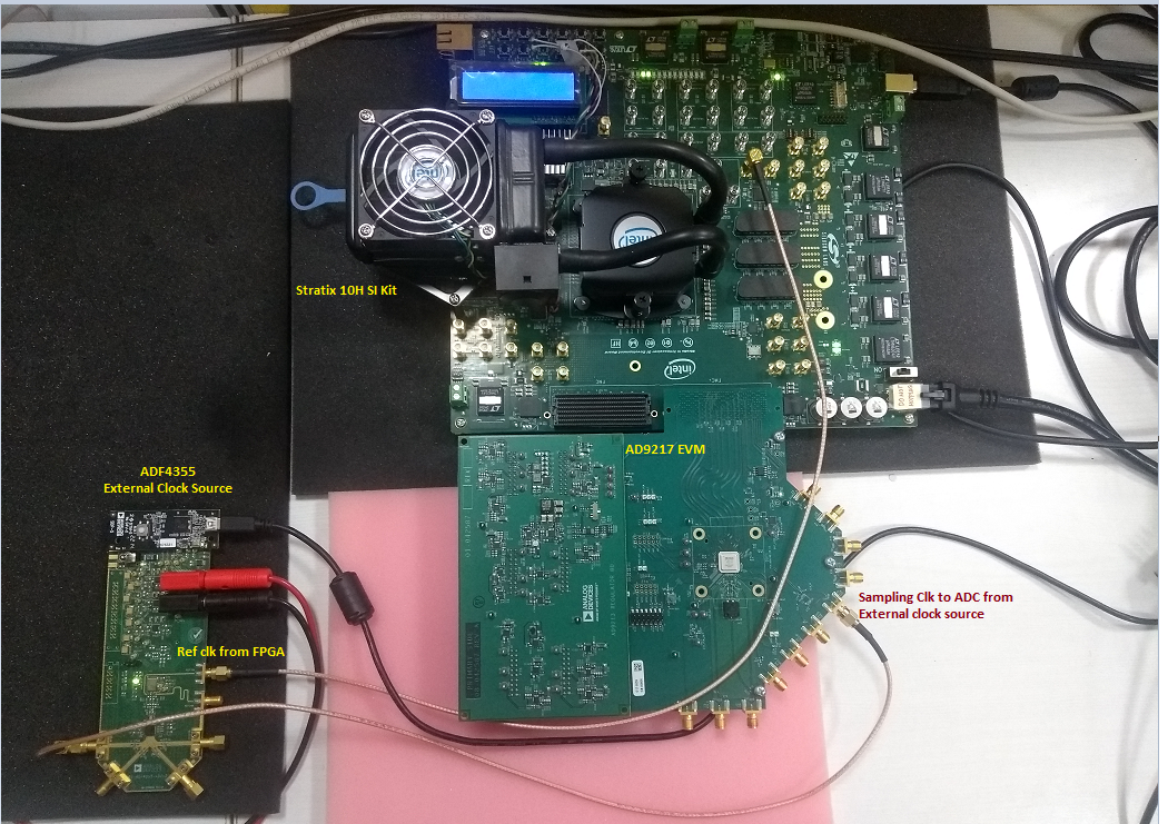
- The ADC AD9217 derives power from the FMC pins.
- The field-programmable gate array (FPGA) device clock is supplied by Si5341 clock generator on the development kit.
- Si5341 clock generator provides reference clock to the ADF4355 clock source and FPGA.
- Sampling clock to the ADC AD9217 EVM is given by the external clock source ADF4355.
The following system-level diagram shows how the different modules connect in this design.
Figure 16. System Diagram—5G Design
In this setup, the data rate of the native PHY transceiver lanes is 5 Gbps. An external clock source card ADF4355 provides sampling clock of 5000 MHz to the ADC (AD9217) through the SMA cables. The Si5341 oscillator on the development kit board provides reference clock to the FPGA and the external clock source board ADF4355. The reference clock to the FPGA is provided to the ATX PLL, which generates the serial clock to transceiver. SPI is used to access the registers in ADC (AD9217).