1. Getting Started
2. Development Kit Overview
3. Power Up the Development Kit
4. Board Test System (BTS)
5. Development Kit Hardware and Configuration
6. Document Revision History for Intel® Stratix® 10 DX FPGA Development Kit User Guide
A. Development Kit Components
B. Safety and Regulatory Information
C. Compliance and Conformity Information
A.1. Components Overview
A.2. Power, Thermal, and Mechanical Considerations
A.3. Clock Circuits
A.4. Memory Interface
A.5. PCIe Interface
A.6. UPI Interface
A.7. Transceiver Signals: PCIe and UPI Interface
A.8. SlimSAS Connector
A.9. QSFP Network Interface
A.10. I2C Interface
A.11. QSPI Flash Memory
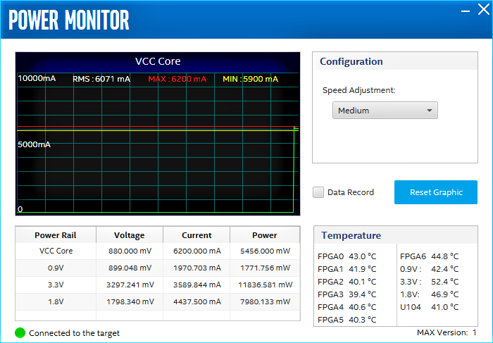
4.3.9. Power Monitor
The Power Monitor measures and reports current power information and communicates with the Intel® MAX® 10 device on the board through the JTAG bus. A power monitor circuit attached to the Intel® MAX® 10 device allows you to measure the power that the Intel® Stratix® 10 DX FPGA is consuming.
To start the application, click the Power Monitor icon in the BTS. You can also run the Power Monitor as a stand-alone application. The PowerMonitor.exe resides in the <package dir>\examples\board_test_system directory.
Note: You cannot run the stand-alone power application and the BTS simultaneously. Also, you cannot run power and clock interface at the same time.
Figure 17. Power Monitor Interface