Video and Vision Processing Suite Intel® FPGA IP User Guide
ID
683329
Date
12/31/2023
Public
A newer version of this document is available. Customers should click here to go to the newest version.
1. About the Video and Vision Processing Suite
2. Getting Started with the Video and Vision Processing IPs
3. Video and Vision Processing IPs Functional Description
4. Video and Vision Processing IP Interfaces
5. Video and Vision Processing IP Registers
6. Video and Vision Processing IPs Software Programming Model
7. Protocol Converter Intel® FPGA IP
8. 1D LUT Intel® FPGA IP
9. 3D LUT Intel® FPGA IP
10. AXI-Stream Broadcaster Intel® FPGA IP
11. Bits per Color Sample Adapter Intel FPGA IP
12. Black Level Correction Intel® FPGA IP
13. Black Level Statistics Intel® FPGA IP
14. Chroma Key Intel® FPGA IP
15. Chroma Resampler Intel® FPGA IP
16. Clipper Intel® FPGA IP
17. Clocked Video Input Intel® FPGA IP
18. Clocked Video to Full-Raster Converter Intel® FPGA IP
19. Clocked Video Output Intel® FPGA IP
20. Color Space Converter Intel® FPGA IP
21. Defective Pixel Correction Intel® FPGA IP
22. Deinterlacer Intel® FPGA IP
23. Demosaic Intel® FPGA IP
24. FIR Filter Intel® FPGA IP
25. Frame Cleaner Intel® FPGA IP
26. Full-Raster to Clocked Video Converter Intel® FPGA IP
27. Full-Raster to Streaming Converter Intel® FPGA IP
28. Genlock Controller Intel® FPGA IP
29. Generic Crosspoint Intel® FPGA IP
30. Genlock Signal Router Intel® FPGA IP
31. Guard Bands Intel® FPGA IP
32. Histogram Statistics Intel® FPGA IP
33. Interlacer Intel® FPGA IP
34. Mixer Intel® FPGA IP
35. Pixels in Parallel Converter Intel® FPGA IP
36. Scaler Intel® FPGA IP
37. Stream Cleaner Intel® FPGA IP
38. Switch Intel® FPGA IP
39. Tone Mapping Operator Intel® FPGA IP
40. Test Pattern Generator Intel® FPGA IP
41. Unsharp Mask Intel® FPGA IP
42. Video and Vision Monitor Intel FPGA IP
43. Video Frame Buffer Intel® FPGA IP
44. Video Frame Reader Intel FPGA IP
45. Video Frame Writer Intel FPGA IP
46. Video Streaming FIFO Intel® FPGA IP
47. Video Timing Generator Intel® FPGA IP
48. Vignette Correction Intel® FPGA IP
49. Warp Intel® FPGA IP
50. White Balance Correction Intel® FPGA IP
51. White Balance Statistics Intel® FPGA IP
52. Design Security
53. Document Revision History for Video and Vision Processing Suite User Guide
28.4.1. Achieving Genlock Controller Free Running (for Initialization or from Lock to Reference Clock N)
28.4.2. Locking to Reference Clock N (from Genlock Controller IP free running)
28.4.3. Setting the VCXO hold over
28.4.4. Restarting the Genlock Controller IP
28.4.5. Locking to Reference Clock N New (from Locking to Reference Clock N Old)
28.4.6. Changing to Reference Clock or VCXO Base Frequencies (switch between p50 and p59.94 video formats and vice-versa)
28.4.7. Disturbing a Reference Clock (a cable pull)
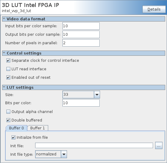
9.2. 3D LUT IP Parameters
The 3D LUT IP offers compile-time parameters.
| Name | Values | Description |
|---|---|---|
| Video data format | ||
| Number of pixels in parallel | 1 to 8 | Number of pixels transmitted every clock cycle. |
| Input bits per color sample | 8 to 16 | Number of bits per color sample at the input. |
| Output bits per color sample | 8 to 16 | Number of bits per color sample at the output. |
| Control settings | ||
| Separate clock for control interface | On or off | Turn on to run the run-time control interface on a different clock domain. |
| LUT read interface | On or off | Allows you to read LUT contents via the CPU interface. |
| Enabled out of reset | On or off |
|
| LUT settings | ||
| Size | 9, 17, 33, 65 | Size of each LUT dimension. |
| Bits per color | 8 to 16 | The number of bits per color in the LUT (LUT_DEPTH). |
| Output alpha channel | On or off | Turn on to add alpha channel to the LUT (RGBA). |
| Bypass alpha | 0 to 2 LUT_DEPTH -1 | The alpha value output in bypass mode. |
| Double buffered | On or off | Double the memory for seamless LUT programming and switching:
|
| Buffer 0 and Buffer 1 | ||
| Initialize from file | On or off | Turn on to initialize the LUT from the initialization file. |
| Init file | user file | Optional initialization file. |
| Init file type | normalized, integer | Type of coefficients in the initialization file:
|
Figure 14. 3D LUT GUI
LUT Initialization File
You can initialize each buffer of the LUT from reset by providing a compatible 3D LUT file to Init file in the GUI. The IP generation process converts the LUT file into RAM initialization .hex files that get built into the firmware during compilation. The script can read .cube format files, or any 3D LUT files that follow these conventions:
- RGB component order (must match the video stream’s order)
- Components change first from left to right, i.e. R first, G second, B third
- If you turn on alpha, you append the alpha value as a fourth component (RGBA)
- The data type must match the IP GUI parameter and may either be:
- normalized fixed- or floating-point numbers between 0.0 to 1.0
- integers between 0 and 2LUT_DEPTH-1 (e.g. 10-bit: 0 to 1023)
- The data type must be the same for the whole file
- Lines starting with # or any letter are ignored