AN 750: Using the Altera PDN Tool to Optimize Your Power Delivery Network Design
1.6.5. Moving Supplies to Optimal Layers
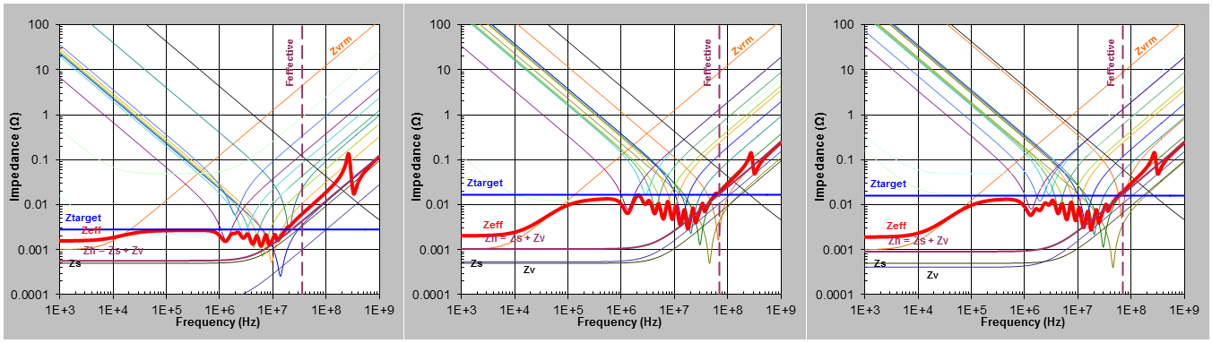
Reducing the spreading inductance (Ls) between the planes and the FPGA increases the effective frequency of the VCC supply. Re-allocating the FPGA supply rails in the layer-stack so that they have lower vertical inductance, will also show an improvement.
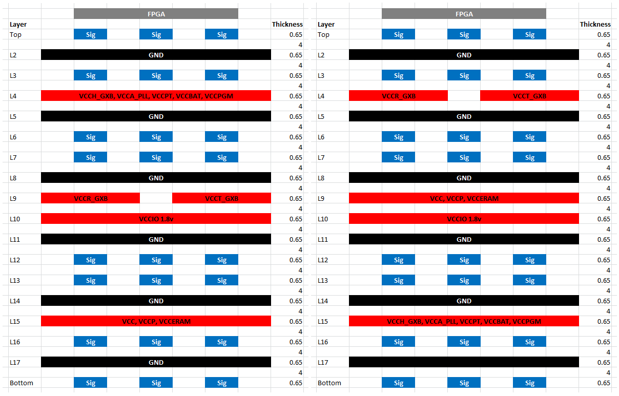
Moving the VCCT_GXB and VCCR GXB supplies from Layer 9 to Layer 4, and the VCC supply from Layer 15 to Layer 9, brings them closer to the FPGA with a lower vertical loop inductance.
The following figure shows a comparison between the initial supply layer allocation on the left with the new allocation on the right.
As a result of these changes, the PDN Tool reports that the VCC supply Feffective has improved from 30.68MHz to 35.61MHz.

The following figure shows that VCCT_GXB and VCCR_GXB supply impedances are close to meeting the 70MHz target. However, further optimization is required because more than 301 capacitors are still required for each of the three supplies.