AN 750: Using the Altera PDN Tool to Optimize Your Power Delivery Network Design
1.6.4. Corrected Number of Power/Ground Via Pairs and Layer Numbers
You should use the correct number of power and ground via pairs for your device. This can be found in the device pinout data. This example uses an AX115N_F45 device selection from the PDN Tool and the initial power plane allocation, the Number of Power/Ground Via Pairs and Layer Number data is corrected and entered into the PDN Tool as shown below:
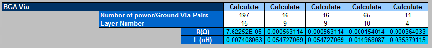
With the corrected Number of Power/Ground Via Pairs and Layer Number data, the total number of required decoupling capacitors remains at 301 for the VCC, VCCT_GXB and VCCR_GXB supplies. The VCC, VCCT_GXB, and VCCR_GXB Impedance plots are shown below.
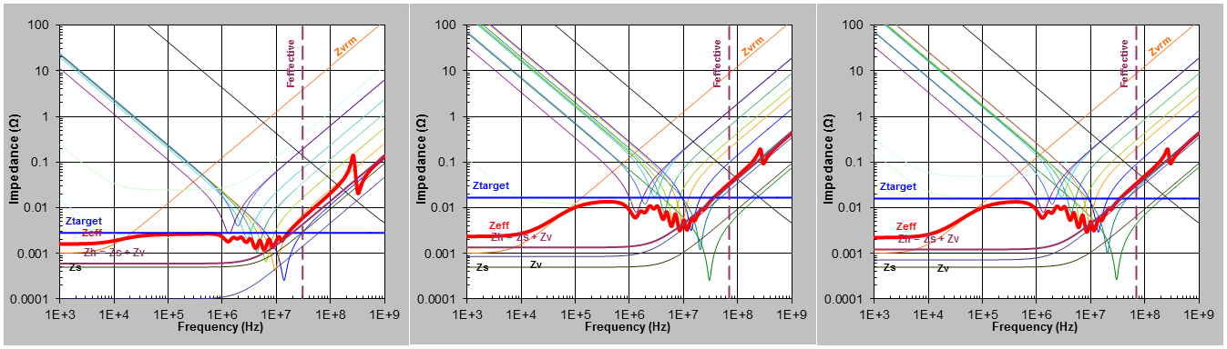
The following figure shows that the VCC supply Feffective parameter has increased from 10.62MHz to 30.68MHz. The increase in performance is due to an increase in the number of power/ground vias from 50 to 197, and a reduction in spreading inductance (Ls). The vertical loop inductance is reduced by moving the VCC supply plane closer to the FPGA from Layer 18 to Layer 15.

In contrast, the VCCT_GXB and VCCR_GXB supply impedance plots shows a lower frequency Zeffective and Ztarget intersect and hence worse PDN performance. This is because the Number of Power/Ground Via Pairs was corrected from 50 to 16 and the spreading inductance increased. The reduction in performance is despite the planes moving closer to the FPGA from Layer 18 to Layer 9, resulting in a reduction in vertical loop inductance.