AN 750: Using the Altera PDN Tool to Optimize Your Power Delivery Network Design
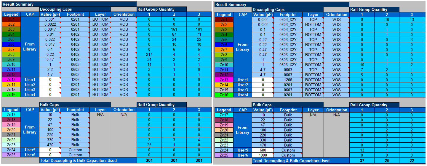
1.6.13. Overall Design Study Capacitor Savings
| PDN Design Stage |
VCC Feffective (MHz) |
VCC Caps Required |
VCCR_GXB Caps |
VCCT_GXB Caps |
|---|---|---|---|---|
| Original stackup, all supplies on L18, # PWR/GND vias = 50 |
10.62 |
>301 |
>301 |
>301 |
| Corrected # PWR/GND vias and layer number Reduced spreading inductance for VCC Increased spreading inductance for VCCR_GXB & VCCT_GXB Reduced vertical inductance for VCC, VCCR_GXB, VCCT_GX |
30.68 |
>301 |
>301 |
>301 |
| Reduce vertical inductance by moving supplies to more optimal layers closer to the FPGA |
35.61 |
>301 |
>301 |
>301 |
| Increase high-frequency capacitance by moving planes closer together |
36.71 |
>301 |
>301 |
239 |
| Reduce vertical inductance by placing decoupling capacitors on top surface |
36.71 |
>301 |
255 |
180 |
| Reduce capacitor mounting inductance by using low ESL X2Y caps |
36.71 |
>301 |
28 |
22 |
| Improve low-frequency performance by using low ESR bulk caps |
36.71 |
>301 |
23 |
17 |
| De-rate VCC high-frequency requirement by using the Core Clock Frequency and Current Ramp Up Period parameters |
36.71 |
37 |
23 |
17 |
The diagrams below compare the original (left) and final (right) PDN Tool number of required capacitors for the VCC, VCCT_GXB, and VCCR_GXB supplies.
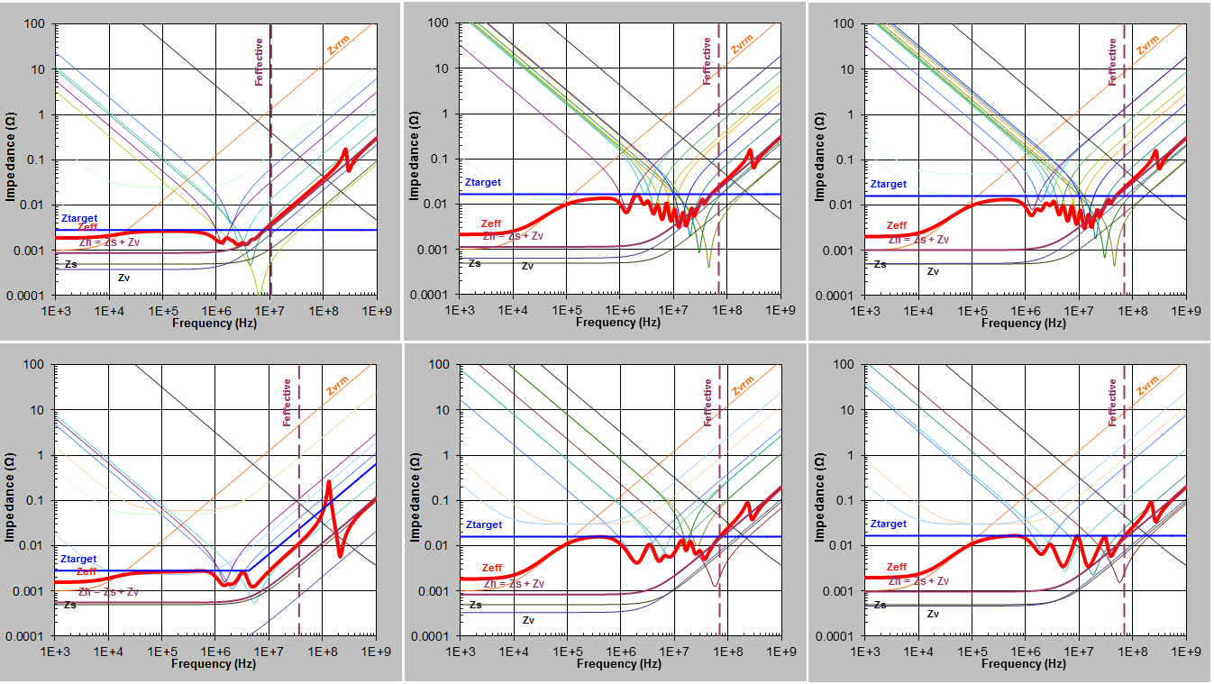
The diagrams below compare the performance of the original (top row) and final (bottom row) PDN performance of the VCC, VCCT_GXB, and VCCR_GXB supplies.