1.5. Example Design
A Quartus project targeting an Arria 10 10AX115N4F45I3SGE2 device, implementing a transceiver design and core noise generators was used to produce current requirements for the core VCC, and transceiver VCCT_GXB and VCCR_GXB supplies.
The following figure shows the transceiver channel placement of the design used in this application note.
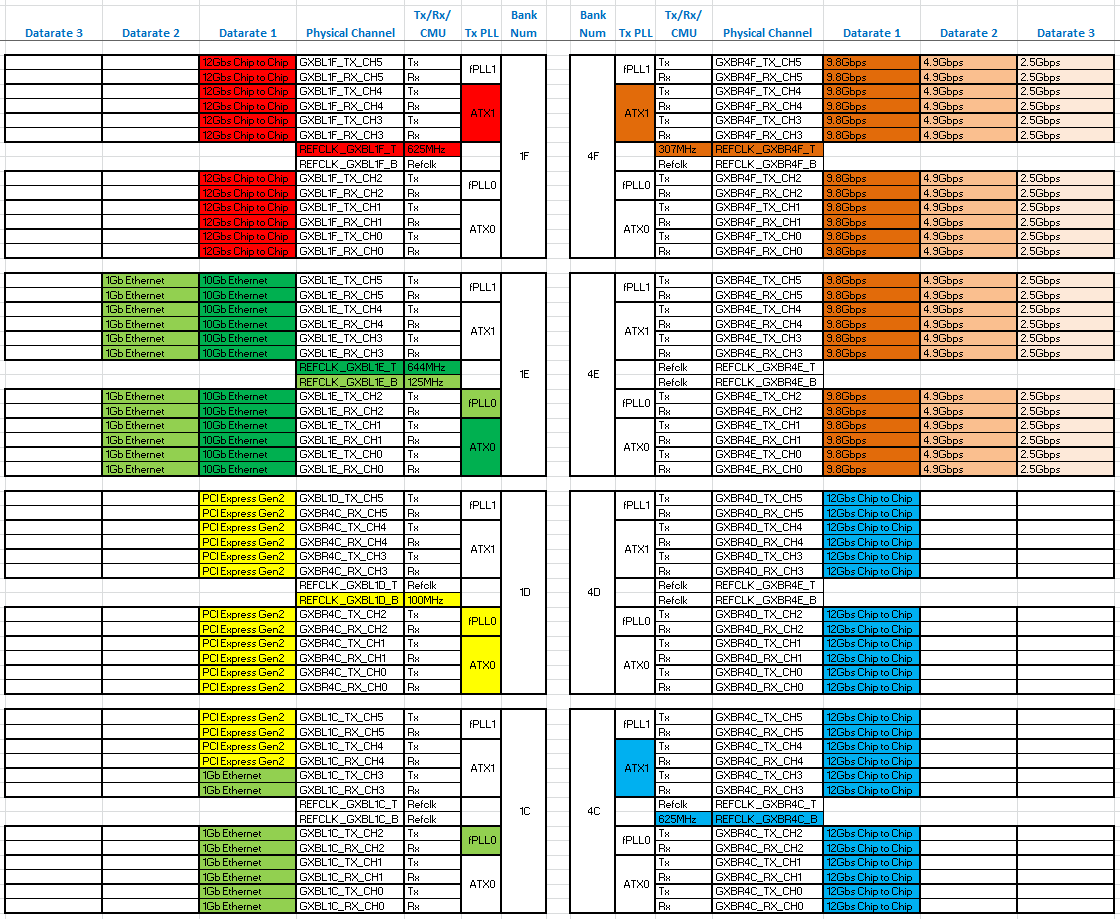
The 1GbE and 10GbE capable channels in transceiver block 1E implement transceiver PHYs capable of switching between the Standard PCS (configured for 1.25 Gbps), and the Enhanced PCS (configured for 10.3125 Gbps). To assess worst case transceiver VCCT_GXB, and VCCR_GXB current requirements, the Enhanced PCS (configured for 10.3125 Gbps) is the default PHY configuration.
The 9.8 Gbps, 4.9 Gbps, 2.5 Gbps capable channels in transceiver blocks 4E and 4F are implemented using the Standard PCS. To assess worst case power requirements of these transceiver blocks, the transceiver PHY default configuration is 9.8 Gbps.
DFE and AEQ were not used for any channels in this design.
Multiple clock pattern and PRBS core noise generators filling 83% of the device logic were implemented for this design. Vectorless estimation was used to generate the PowerPlay Power Analyzer results.
You should base your power requirement estimates on your actual design.
| Power Supply Pin |
Voltage(V) |
Current (mA) |
Power Group |
|---|---|---|---|
| VCC |
0.9 |
32000.00 |
1 |
| VCCP |
0.9 |
13500.00 |
1 |
| VCCERAM |
0.9 |
0.045 |
1 |
| VCCR_GXBL1C |
1.0 |
224.09 |
3 |
| VCCR_GXBL1D |
1.0 |
403.75 |
3 |
| VCCR_GXBL1E |
1.0 |
991.02 |
3 |
| VCCR_GXBL1F |
1.0 |
1021.69 |
3 |
| VCCR_GXBR4C |
1.0 |
944.15 |
3 |
| VCCR_GXBR4D |
1.0 |
955.29 |
3 |
| VCCR_GXBR4E |
1.0 |
667.44 |
3 |
| VCCR_GXBR4F |
1.0 |
757.41 |
3 |
| VCCT_GXBL1C |
1.0 |
56.42 |
2 |
| VCCT_GXBL1D |
1.0 |
78.86 |
2 |
| VCCT_GXBL1E |
1.0 |
297.65 |
2 |
| VCCT_GXBL1F |
1.0 |
372.85 |
2 |
| VCCT_GXBR4C |
1.0 |
356.23 |
2 |
| VCCT_GXBR4D |
1.0 |
356.23 |
2 |
| VCCT_GXBR4E |
1.0 |
281.97 |
2 |
| VCCT_GXBR4F |
1.0 |
298.58 |
2 |
The current estimates from the above table were entered in the PDN Tool as shown below:
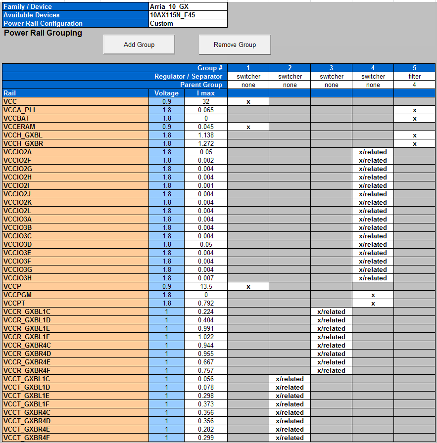
Because of the high number of channels clocked from single ATX PLLs x/related is chosen for the VCCT_GXB and VCCR_GXB supplies in this design. With the x/related setting, the PDN Tool assumes the supplies have synchronous switching and hence higher dynamic current. This makes the PDN design more challenging, but is a worst case scenario as not all channels are synchronous. Assess if you should select x or x/related for your design.