LVDS SERDES Transmitter / Receiver IP Cores User Guide
1.5.5. Arria II GX, Arria® V, Arria® V GZ, Cyclone® V, and Stratix® V LVDS Package Skew Compensation Report Panel
This section describes the LVDS package skew compensation report panel for the transmitter and non-DPA receiver of the Arria II GX, Arria® V, Arria® V GZ, Cyclone® V, and Stratix® V device families.
The report panel contains details about the package trace delay compensation needed between the LVDS pins on the device to meet your timing budget. You can find the report panel in the Intel® Quartus® Prime Fitter report under Resource Section. The report panel is called LVDS Receiver Package Skew Compensation, and LVDS Transmitter Package Skew Compensation for the LVDS receiver and LVDS transmitter respectively. The report panel is triggered in the Intel® Quartus® Prime software when your design uses a non-DPA receiver, and with an input data rate higher than 840 Mbps.
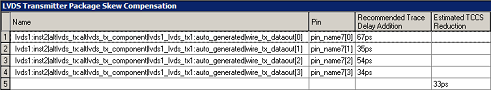
The following figure shows the LVDS Transmitter Package Skew Compensation report panel.
The following figure shows the LVDS Receiver Package Skew Compensation report panel.
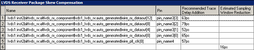
The Recommended Trace Delay Addition column in the report panel displays the recommended amount of trace delay that you must add to each trace of the corresponding LVDS pins, which reduces the channel-to-channel skew between the LVDS channels. For example, in Figure 6, the recommended trace delay addition for pin_name7[0] is 67 ps. This means you must manually adjust the PCB trace for pin_name7[0] to have a delay addition of 67 ps. The corresponding pin is listed in the Pin column, in the report panel.
The report panel also shows the total estimated TCCS and SW reductions when the recommended trace delay values are added to the PCB trace.