1.4. Compiling and Testing the SDI II Design Example in Hardware
- For the Agilex 5 FPGA E-Series 065B Premium Development Kit:
Figure 6. Agilex 5 Premium Development Kit Clock Controller
- For the Agilex 5 FPGA E-Series 065B Modular Development Kit:
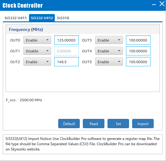
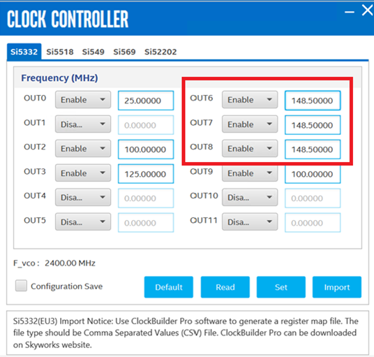
- On the SI5332 tab, set OUT6 - OUT8 to 148.5
Figure 7. Set SI5332
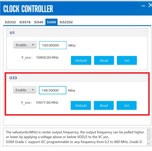
- On the SI569 tab, set U33 to 148.5
Figure 8. Set SI569
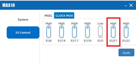
- On the MAX10 tab, click IO Control and Clock Mux tab, and set EU21 to High (default is low).
Figure 9. Set EU21
- On the SI5332 tab, set OUT6 - OUT8 to 148.5
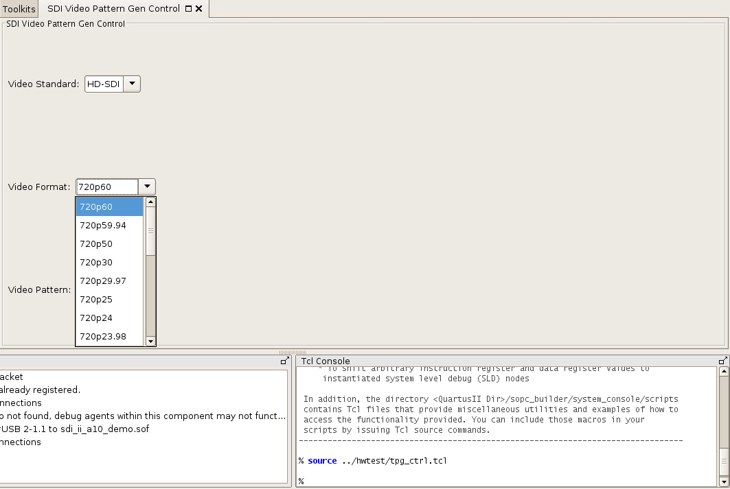
- For serial loopback designs, open System Console to control the internal video pattern generator:
- Select your desired video format through the GUI.
To allow segmented frame video formats (1080sF30, 1080sF25) and interlaced video formats (1080i60, 1080i50) to be correctly differentiated in an external analyzer, insert payload ID in the serial loopback design.Figure 10. Selecting Video Format Through System Console
- Select your desired video format through the GUI.
- The analyzer should be able to display the video generated from the source. Refer to jumper settings in the Jumper Settings and Descriptions table to change the jumper (J8) position before switching between fractional frame rate and integer frame rate video format. Press the push button (PB0) to trigger a device (LMK03328) power cycling through the PDN pin every time you change the jumper (J8) position.
Figure 11. Jumper Settings on Nextera 12G-SDI FMC Daughtercard
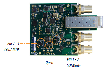
Table 3. Jumper Settings and Descriptions Jumper Block Description Setting J7 Programming Header - J8 To switch the generated clock frequency to TX channel:
- Pin 1-2 = 297 MHz
- Pin 2-3 = 297/1.001 MHz
1-2: 297 MHz 2-3: 297/1.001 MHz
J9 To select SDI or IP mode:
- Pin 1-2 = SDI mode
- Pin 2-3 = IP mode
1-2