4.4. Simulating the Design Example
- Change to the testbench simulation directory, intel_pcie_ptile_avmm_0_example_design\pcie_ed_tb.
- Run the simulation script for VCS. Refer to the table below.
- Analyze the results.
| Simulator | Working Directory | Instructions |
|---|---|---|
| VCS* | <example_design>/pcie_ed_tb/pcie_ed_tb/sim/synopsys/vcs |
Note:
To run a simulation in interactive mode, use the following steps: (if you already generated a simv executable in non-interactive mode, delete the simv and simv.diadir)
|
- Writes to the Endpoint memory using the DUT Endpoint non-bursting Avalon® -MM master interface.
- Reads from Endpoint memory using the DUT Endpoint non-bursting Avalon® -MM master interface.
- Verifies the data using the shmem_chk_ok task.
- Writes to the Endpoint DMA controller, instructing the DMA controller to perform a MRd request to the PCIe* address space in host memory.
- Writes to the Endpoint DMA controller, instructing the DMA controller to perform a MWr request to PCIe* address space in host memory. This MWr uses the data from the previous MRd.
- Verifies the data using the shmem_chk_ok task.
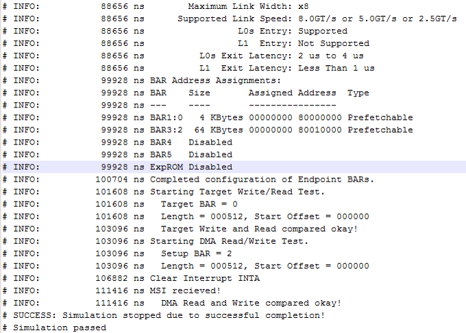
The simulation reports, "Simulation stopped due to successful completion" if no errors occur.
The following figure shows the behavior of Data Mover interface signals during a read data transfer followed by a write data transfer.
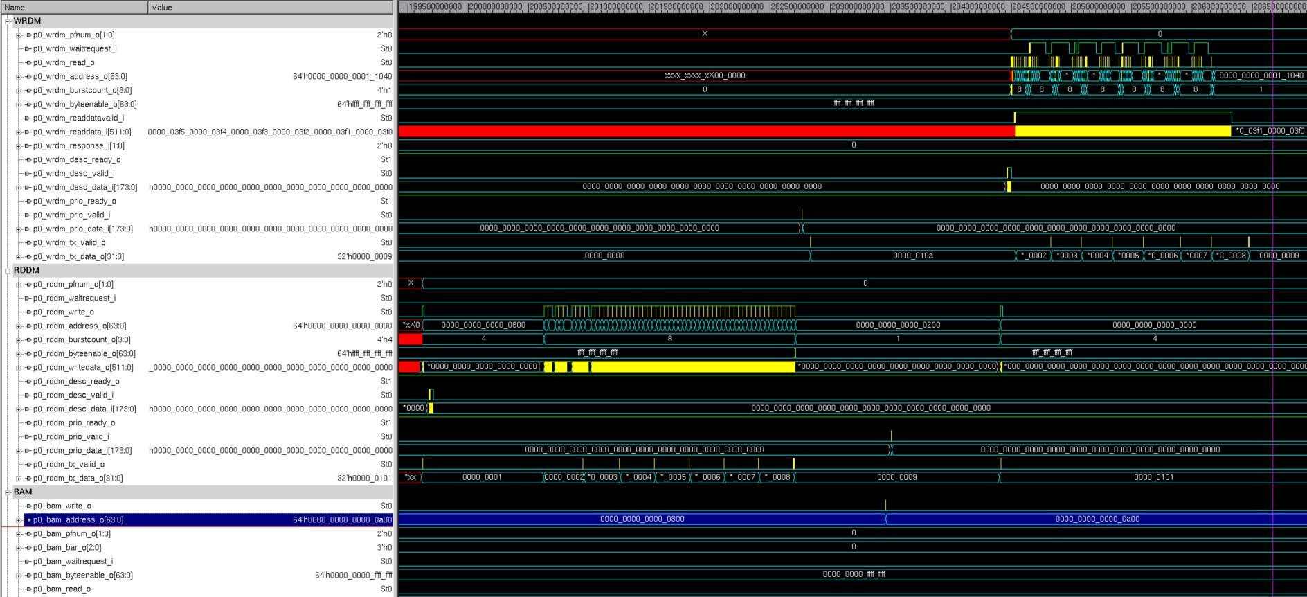
As shown in the simulation waveforms, the Read Data Mover's data transfer happened around 200 us, and the Write Data Mover's data transfer happened around 204 us.
Test Case for the Endpoint Gen4 x16 Design Example
The test case for this design example is in the file intel_pcie_ptile_avmm_0_example_design\pcie_ed_tb\ip\pcie_ed_tb\dut_pcie_tb_ip\intel_pcie_ptile_tbed_100\sim\altpcietb_bfm_rp_gen4_x16.sv.
The task to run the test is called avmmdma_rdwr_512IP_test.
The test case consists of:
- Create a Ramp in Buffer_0.
- Create an associated descriptor table targeting Buffer_0.
- Create a descriptor for the read descriptor table (created in step 2) and append a descriptor to write to the host memory when DMA is done.
- Send the descriptor (created in step 3) to the DMA controller through the BAM Interface.
- The DMA Controller processes the descriptor then reads the descriptor tables. At this time, all descriptors are fetched and placed inside the DMA Controller FIFO.
- The Read Data Mover issues a read command to read data from Buffer_0 and send it to the internal RAM.
- The Read Data Mover issues a MWr for the Status bit.
- Create an empty Buffer_1.
- Create an associated descriptor table targeting Buffer_1.
- Create a descriptor for the read descriptor table (created in step 2) and append a descriptor to write to the host memory when DMA is done.
- Send the descriptor (created in step 3) to the DMA controller through the BAM Interface.
- The DMA Controller processes the descriptor then reads the descriptor tables. At this time, all descriptors are fetched and placed inside the DMA Controller FIFO.
- The Write Data Mover issues a read command to read data from internal RAM and send it to the PCIe host memory.
- The Write Data Mover issues a MWr for the Status bit.
The test case then compares the contents of Buffer_0 and Buffer_1. If they match, the test passes.