Arria V Avalon-ST Interface for PCIe Solutions User Guide
ID
683733
Date
6/03/2020
Public
A newer version of this document is available. Customers should click here to go to the newest version.
1. Datasheet
2. Getting Started with the Arria V Hard IP for PCI Express
3. Parameter Settings
4. Interfaces and Signal Descriptions
5. Registers
6. Interrupts
7. Error Handling
8. IP Core Architecture
9. Transaction Layer Protocol (TLP) Details
10. Throughput Optimization
11. Design Implementation
12. Additional Features
13. Hard IP Reconfiguration
14. Transceiver PHY IP Reconfiguration
15. Testbench and Design Example
16. Debugging
A. Transaction Layer Packet (TLP) Header Formats
B. Lane Initialization and Reversal
C. Document Revision History
1.1. Arria V Avalon-ST Interface for PCIe Datasheet
1.2. Features
1.3. Release Information
1.4. Device Family Support
1.5. Configurations
1.6. Example Designs
1.7. Debug Features
1.8. IP Core Verification
1.9. Performance and Resource Utilization
1.10. Recommended Speed Grades
1.11. Creating a Design for PCI Express
4.1. Arria V Hard IP for PCI Express with Avalon-ST Interface to the Application Layer
4.2. Clock Signals
4.3. Reset Signals
4.4. Hard IP Status
4.5. Error Signals
4.6. ECRC Forwarding
4.7. Interrupts for Endpoints
4.8. Interrupts for Root Ports
4.9. Completion Side Band Signals
4.10. Transaction Layer Configuration Space Signals
4.11. LMI Signals
4.12. Power Management Signals
4.13. Physical Layer Interface Signals
5.1. Correspondence between Configuration Space Registers and the PCIe Specification
5.2. Type 0 Configuration Space Registers
5.3. Type 1 Configuration Space Registers
5.4. PCI Express Capability Structures
5.5. Intel-Defined VSEC Registers
5.6. CvP Registers
5.7. Uncorrectable Internal Error Mask Register
5.8. Uncorrectable Internal Error Status Register
5.9. Correctable Internal Error Mask Register
5.10. Correctable Internal Error Status Register
15.6.1. ebfm_barwr Procedure
15.6.2. ebfm_barwr_imm Procedure
15.6.3. ebfm_barrd_wait Procedure
15.6.4. ebfm_barrd_nowt Procedure
15.6.5. ebfm_cfgwr_imm_wait Procedure
15.6.6. ebfm_cfgwr_imm_nowt Procedure
15.6.7. ebfm_cfgrd_wait Procedure
15.6.8. ebfm_cfgrd_nowt Procedure
15.6.9. BFM Configuration Procedures
15.6.10. BFM Shared Memory Access Procedures
15.6.11. BFM Log and Message Procedures
15.6.12. Verilog HDL Formatting Functions
15.7.1. Changing Between Serial and PIPE Simulation
15.7.2. Using the PIPE Interface for Gen1 and Gen2 Variants
15.7.3. Viewing the Important PIPE Interface Signals
15.7.4. Disabling the Scrambler for Gen1 and Gen2 Simulations
15.7.5. Disabling 8B/10B Encoding and Decoding for Gen1 and Gen2 Simulations
15.7.6. Changing between the Hard and Soft Reset Controller
2.1. Qsys Design Flow
Copy the pcie_de_gen1_x4_ast64.qsys design example from the <install_dir>/ip/altera/altera_pcie/altera_pcie/altera_pcie_hip_ast_ed/example_designs/<dev> to your working directory. The following figure illustrates this Qsys system.
Figure 7. Complete Gen1 ×4 Endpoint (DUT) Connected to Example Design (APPS)
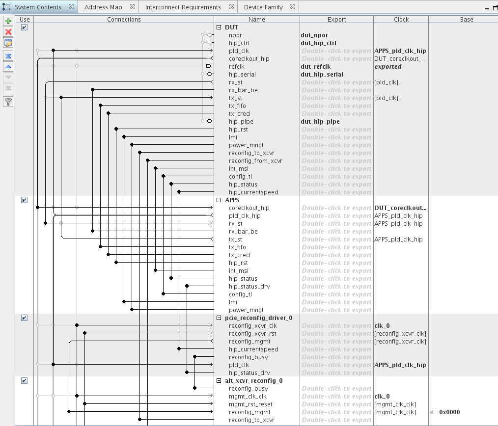
The example design includes the following components:
- DUT—This is Gen1 ×4 Endpoint. For your own design, you can select the data rate, number of lanes, and either Endpoint or Root Port mode.
- APPS—This DMA driver configures the DUT and drives read and write TLPs to test DUT functionality.
- pcie_reconfig_driver_0—This Avalon‑MM master drives the Transceiver Reconfiguration Controller. The pcie_reconfig_driver_0 is implemented in clear text that you can modify if your design requires different reconfiguration functions. After you generate your Qsys system, the Verilog HDL for this component is available as: <working_dir>/<variant_name>/testbench/<variant_name>_tb/simulation/submodules/altpcie_reconfig_driver.sv.
- Transceiver Reconfiguration Controller—The Transceiver Reconfiguration Controller dynamically reconfigures analog settings to improve signal quality. For Gen1 and Gen2 data rates, the Transceiver Reconfiguration Controller must perform offset cancellation and PLL calibration.