AN 706: Routing HPS Peripheral Signals to the FPGA External Interface
1.2.3. Generating the Initial HDL in Platform Designer (Standard)
- In the Intel® Quartus® Prime Standard Edition navigation bar, select Tools > Platform Designer (Standard) .
- In the Platform Designer (Standard) window, select File > Open > soc_system.qsys .
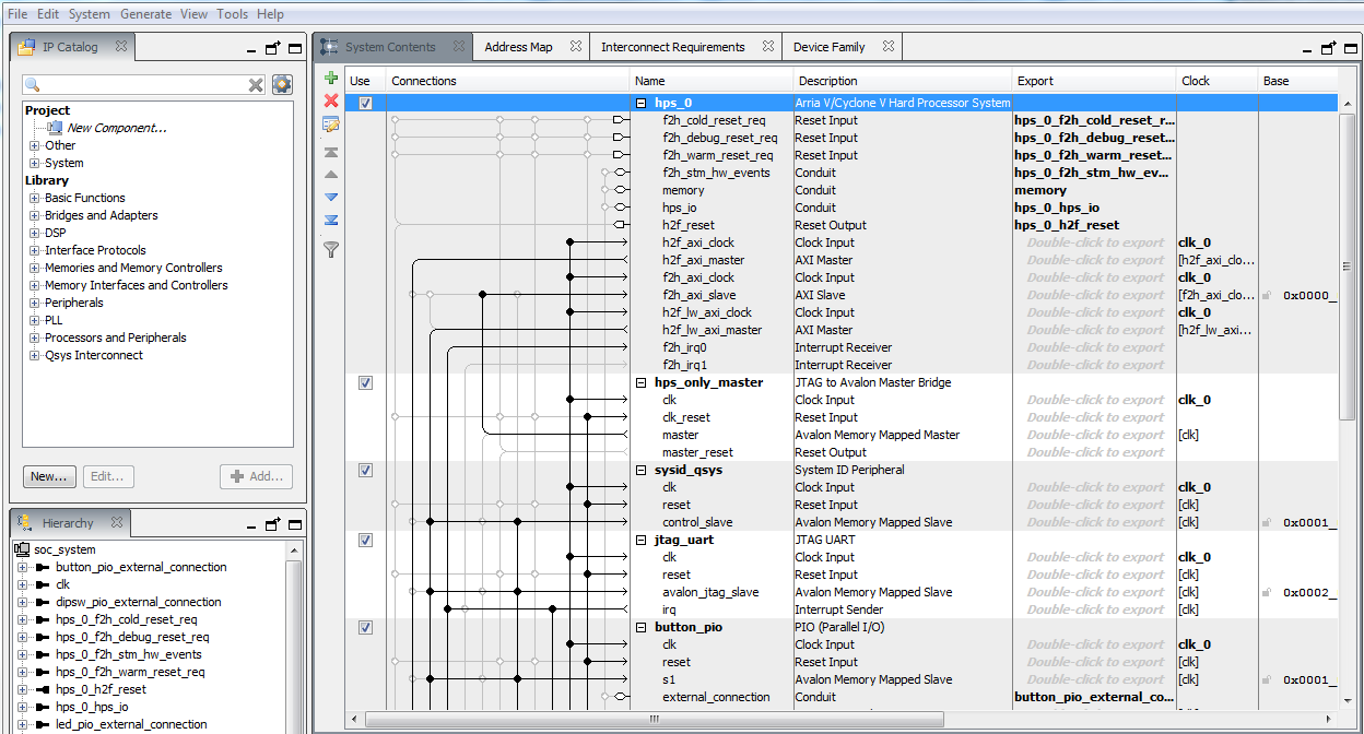
- In the System Contents tab, double click on hps_0 to open the HPS Parameters window.
Figure 2. System Contents Window

- On the Peripheral Pins tab, under the Ethernet Media Access Controller section, click on the EMAC0 pin pull-down and select FPGA. The EMAC0 mode pull-down automatically displays Full to indicate GMII mode. Select the EMAC1 pin pull-down as Unused.
Figure 3. Selecting FPGA for EMAC0 Pin in the HPS Parameters Window

- On the Peripheral Pins tab, scroll down to the I2C Controllers section, click on the I2C0 pin pull-down and select FPGA. The I2C0 mode pull-down automatically displays Full.
Figure 4. Selecting FPGA for I2C0 Pin in the HPS Parameters Window

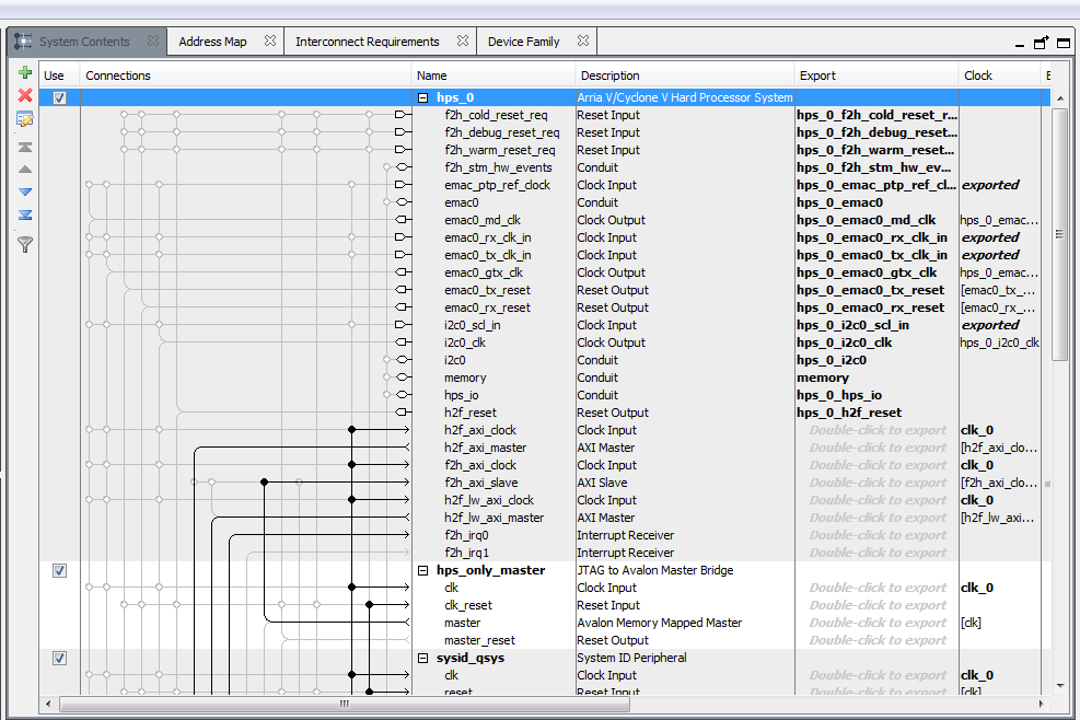
- Return to the System Contents tab and in the Export column, double-click on the EMAC0 and I2C0 signal pins to export them as conduits.
Figure 5. Exporting Pins in System Contents Window

- Select Generate > Generate HDL from the Platform Designer (Standard) menu bar. In the project directory, replace the top level RTL file, ghrd_top.v, with the generated Verilog file.
Platform Designer (Standard) exposes the following EMAC0 and I2C0 interfaces in the file:
Table 3. EMAC0 Signals in the FPGA Domain Signal
Width
Direction
Description
emac0_phy_txd_o
8
Out
PHY Transmit Data
emac0_phy_txen_o
1
Out
PHY Transmit Data Enable
emac0_phy_txer_o
1
Out
PHY Transmit Error
emac0_phy_rxdv_i
1
In
PHY Receive Data Valid
emac0_phy_rxer_i
1
In
PHY Receive Error
emac0_phy_rxd_i
8
In
PHY Receive Data
emac0_phy_col_i
1
In
PHY Collision Detect
emac0_phy_crs_i
1
In
PHY Carrier Sense
emac0_gmii_mdo_o
1
Out
MDIO signal data out
emac0_gmii_mdo_o_e
1
Out
MDIO signal output enable
emac0_gmii_mdi_i
1
In
MDIO signal input
emac0_gmii_mdc_o
1
Out
Management Data Clock
emac0_clk_rx_i
1
In
PHY RX reference clock
emac0_clk_tx_i
1
In
PHY TX reference clock
emac0_phy_txclk_o
1
Out
Transmit clock output to the PHY
emac0_rst_clk_tx_n_o
1
Out
Transmit clock reset output to the FPGA interface
emac0_rst_clk_rx_n_o
1
Out
Receive clock reset output
Table 4. I2C0 Signals in the FPGA Domain Signal
Width
Direction
Description
i2c0_out_data
1
Out
Outgoing I2C data enable
i2c0_sda
1
In
Incoming I2C data
i2c0_clk_clk
1
Out
Outgoing I2C clock enable
i2c0_scl_in_clk
1
In
Incoming I2C clock source