A newer version of this document is available. Customers should click here to go to the newest version.
7.1.3.1. System PLL Clocking Mode
SDI II Intel FPGA IP generated design example uses the System PLL Clocking Mode where the datapath is clocked by one of the 3 on-board system PLLs.
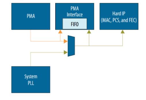
The output frequency of System PLL must be higher than the PMA recovered clock, so that the write-side of the FIFO in Figure 40 always operates in slower clock region than the read-side of the FIFO. This ensures that no data is missed while data transition between these 2 clock domains.
The below table summarizes the minimum System PLL output frequency for different SDI modes:
| SDI Mode | Minimum System PLL Output Frequency |
|---|---|
| HD-SDI single rate | 150 MHz |
| 3G-SDI single rate | 300 MHz |
| 12G-SDI single rate | 600 MHz |
The system PLL output clock can be shared with other protocols. For example, if Ethernet IP requires a higher clock frequency at 800+ MHz, you must configure the System PLL to output a clock at 800+ MHz and share this clock between SDI II IP and Ethernet IP.
Since the datapath on transceiver is now clocked by a higher clock frequency than what is required by SDI II core, a DC FIFO is required to transfer the data back to the slower clock domain required by SDI II core. F-tile PMA/FEC Direct PHY Intel FPGA IP allows you to output 2 recovered clocks, 1 being the (System PLL output)/2 clock, and another 1 being the slower clock required by SDI II core. SDI II IP core expects 148.5 MHz recovered clock from PMA for all data rates, except for HD-SDI which requires 74.25 MHz recovered clock.
Another thing to note is the custom cadence on data validity in the System PLL Clocking Mode. Since the System PLL output clock is running at a higher clock frequency than the real data rate, the data coming out/going into the PHY may not be valid at every clock cycle. On RX side, rx_parallel_data[38] represents the data_valid bit of the recovered data which can be connected to the write request port of the DC FIFO. On TX side, F-tile PMA/FEC Direct PHY IP has a feature to enable custom cadence generation ports and logic. An additional interface port named “tx_cadence” will be introduced when this mode is enabled. This signal indicates the rate at which the data_valid bit on tx_parallel_data must be toggled. Hence, it can serve as the read request port of the DC FIFO interfacing with TX PHY as well as to toggle the data_valid bit on the tx_parallel_data to TX PHY. The following diagrams illustrate the interfacing between PHY, DC FIFO, and SDI IP core.