A newer version of this document is available. Customers should click here to go to the newest version.
1. Introduction
2. Avalon® -ST Multi-Channel Shared Memory FIFO Core
3. Avalon® -ST Single-Clock and Dual-Clock FIFO Cores
4. Avalon® -ST Serial Peripheral Interface Core
5. SPI Core
6. SPI Agent/JTAG to Avalon® Host Bridge Cores
7. Intel eSPI Agent Core
8. eSPI to LPC Bridge Core
9. Ethernet MDIO Core
10. Intel FPGA 16550 Compatible UART Core
11. UART Core
12. JTAG UART Core
13. Intel FPGA Avalon® Mailbox Core
14. Intel FPGA Avalon® Mutex Core
15. Intel FPGA Avalon® I2C (Host) Core
16. Intel FPGA I2C Agent to Avalon® -MM Host Bridge Core
17. Intel FPGA Avalon® Compact Flash Core
18. EPCS/EPCQA Serial Flash Controller Core
19. Intel FPGA Serial Flash Controller Core
20. Intel FPGA Serial Flash Controller II Core
21. Intel FPGA Generic QUAD SPI Controller Core
22. Intel FPGA Generic QUAD SPI Controller II Core
23. Interval Timer Core
24. Intel FPGA Avalon FIFO Memory Core
25. On-Chip Memory (RAM and ROM) Core
26. On-Chip Memory II (RAM or ROM)
27. Optrex 16207 LCD Controller Core
28. PIO Core
29. PLL Cores
30. DMA Controller Core
31. Modular Scatter-Gather DMA Core
32. Scatter-Gather DMA Controller Core
33. SDRAM Controller Core
34. Tri-State SDRAM Core
35. Video Sync Generator and Pixel Converter Cores
36. Intel FPGA Interrupt Latency Counter Core
37. Performance Counter Unit Core
38. Vectored Interrupt Controller Core
39. Avalon® -ST Data Pattern Generator and Checker Cores
40. Avalon® -ST Test Pattern Generator and Checker Cores
41. System ID Peripheral Core
42. Avalon® Packets to Transactions Converter Core
43. Avalon® -ST Multiplexer and Demultiplexer Cores
44. Avalon® -ST Bytes to Packets and Packets to Bytes Converter Cores
45. Avalon® -ST Delay Core
46. Avalon® -ST Round Robin Scheduler Core
47. Avalon® -ST Splitter Core
48. Avalon® -MM DDR Memory Half Rate Bridge Core
49. Intel FPGA GMII to RGMII Converter Core
50. Intel FPGA MII to RMII Converter Core
51. Intel FPGA HPS GMII to TSE 1000BASE-X/SGMII PCS Bridge Core
52. Intel FPGA HPS EMAC to Multi-rate PHY GMII Adapter Core
53. Intel FPGA MSI to GIC Generator Core
10.2.1. Unsupported Features
10.2.2. Interface
10.2.3. General Architecture
10.2.4. 16550 UART General Programming Flow Chart
10.2.5. Configuration Parameters
10.2.6. DMA Support
10.2.7. FPGA Resource Usage
10.2.8. Timing and Fmax
10.2.9. Avalon® -MM Agent
10.2.10. Over-run/Under-run Conditions
10.2.11. Hardware Auto Flow-Control
10.2.12. Clock and Baud Rate Selection
15.5.2.1. Transfer Command FIFO (TFR_CMD)
15.5.2.2. Receive Data FIFO (RX_DATA)
15.5.2.3. Control Register (CTRL)
15.5.2.4. Interrupt Status Enable Register (ISER)
15.5.2.5. Interrupt Status Register (ISR)
15.5.2.6. Status Register (STATUS)
15.5.2.7. TFR CMD FIFO Level (TFR CMD FIFO LVL)
15.5.2.8. RX Data FIFO Level (RX Data FIFO LVL)
15.5.2.9. SCL Low Count (SCL LOW)
15.5.2.10. SCL High Count (SCL HIGH)
15.5.2.11. SDA Hold Count (SDA HOLD)
24.6.1. altera_avalon_fifo_init()
24.6.2. altera_avalon_fifo_read_status()
24.6.3. altera_avalon_fifo_read_ienable()
24.6.4. altera_avalon_fifo_read_almostfull()
24.6.5. altera_avalon_fifo_read_almostempty()
24.6.6. altera_avalon_fifo_read_event()
24.6.7. altera_avalon_fifo_read_level()
24.6.8. altera_avalon_fifo_clear_event()
24.6.9. altera_avalon_fifo_write_ienable()
24.6.10. altera_avalon_fifo_write_almostfull()
24.6.11. altera_avalon_fifo_write_almostempty()
24.6.12. altera_avalon_write_fifo()
24.6.13. altera_avalon_write_other_info()
24.6.14. altera_avalon_fifo_read_fifo()
24.6.15. altera_avalon_fifo_read_other_info()
25.1. Core Overview
25.2. Component-Level Design for On-Chip Memory
25.3. Platform Designer System-Level Design for On-Chip Memory
25.4. Simulation for On-Chip Memory
25.5. Intel® Quartus® Prime Project-Level Design for On-Chip Memory
25.6. Board-Level Design for On-Chip Memory
25.7. Example Design with On-Chip Memory
25.8. On-Chip Memory (RAM and ROM) Core Revision History
26.1. Core Overview
26.2. Embedded Memory Architecture and Features
26.3. Component-Level Design for On-Chip Memory II
26.4. Platform Designer System-Level Design for On-Chip Memory II
26.5. Simulation for On-Chip Memory II
26.6. Intel® Quartus® Prime Project-Level Design for On-Chip Memory II
26.7. Board-Level Design for On-Chip Memory II
26.8. Example Design with On-Chip Memory II
26.9. On-Chip Memory II (RAM and ROM) Core Revision History
31.1. Core Overview
31.2. Feature Description
31.3. mSGDMA Interfaces and Parameters
31.4. mSGDMA Descriptors
31.5. Register Map of mSGDMA
31.6. Programming Model
31.7. Modular Scatter-Gather DMA Prefetcher Core
31.8. Driver Implementation
31.9. Example Code Using mSGDMA Core
31.10. Modular Scatter-Gather DMA Core Revision History
31.5.1. Status Register
31.5.2. Control Register
31.5.3. Write Fill Level Register
31.5.4. Read Fill Level Register
31.5.5. Response Fill Level Register
31.5.6. Write Sequence Number Register
31.5.7. Read Sequence Number Register
31.5.8. Component Configuration 1 Register
31.5.9. Component Configuration 2 Register
31.5.10. Component Type Register
31.5.11. Component Version Register
31.8.1. alt_msgdma_standard_descriptor_async_transfer
31.8.2. alt_msgdma_extended_descriptor_async_transfer
31.8.3. alt_msgdma_descriptor_async_transfer
31.8.4. alt_msgdma_standard_descriptor_sync_transfer
31.8.5. alt_msgdma_extended_descriptor_sync_transfer
31.8.6. alt_msgdma_descriptor_sync_transfer
31.8.7. alt_msgdma_construct_standard_st_to_mm_descriptor
31.8.8. alt_msgdma_construct_standard_mm_to_st_descriptor
31.8.9. alt_msgdma_construct_standard_mm_to_mm_descriptor
31.8.10. alt_msgdma_construct_standard_descriptor
31.8.11. alt_msgdma_construct_extended_st_to_mm_descriptor
31.8.12. alt_msgdma_construct_extended_mm_to_st_descriptor
31.8.13. alt_msgdma_construct_extended_mm_to_mm_descriptor
31.8.14. alt_msgdma_construct_extended_descriptor
31.8.15. alt_msgdma_register_callback
31.8.16. alt_msgdma_open
31.8.17. alt_msgdma_write_standard_descriptor
31.8.18. alt_msgdma_write_extended_descriptor
31.8.19. alt_msgdma_init
31.8.20. alt_msgdma_irq
32.7.1. Data Structure
32.7.2. SG-DMA API
32.7.3. alt_avalon_sgdma_do_async_transfer()
32.7.4. alt_avalon_sgdma_do_sync_transfer()
32.7.5. alt_avalon_sgdma_construct_mem_to_mem_desc()
32.7.6. alt_avalon_sgdma_construct_stream_to_mem_desc()
32.7.7. alt_avalon_sgdma_construct_mem_to_stream_desc()
32.7.8. alt_avalon_sgdma_enable_desc_poll()
32.7.9. alt_avalon_sgdma_disable_desc_poll()
32.7.10. alt_avalon_sgdma_check_descriptor_status()
32.7.11. alt_avalon_sgdma_register_callback()
32.7.12. alt_avalon_sgdma_start()
32.7.13. alt_avalon_sgdma_stop()
32.7.14. alt_avalon_sgdma_open()
38.5.6.1. altera_vic_driver.enable_preemption
38.5.6.2. altera_vic_driver.enable_preemption_into_new_register_set
38.5.6.3. altera_vic_driver.enable_preemption_rs_<n>
38.5.6.4. altera_vic_driver.linker_section
38.5.6.5. altera_vic_driver.<name>.vec_size
38.5.6.6. altera_vic_driver.<name>.irq<n>_rrs
38.5.6.7. altera_vic_driver.<name>.irq<n>_ril
38.5.6.8. altera_vic_driver.<name>.irq<n>_rnmi
38.5.6.9. Default Settings for RRS and RIL
38.5.6.10. VIC BSP Design Rules for Intel FPGA HAL Implementation
38.5.6.11. RTOS Considerations
40.1. Core Overview
40.2. Resource Utilization and Performance
40.3. Test Pattern Generator
40.4. Test Pattern Checker
40.5. Hardware Simulation Considerations
40.6. Software Programming Model
40.7. Test Pattern Generator API
40.8. Test Pattern Checker API
40.9. Avalon® -ST Test Pattern Generator and Checker Cores Revision History
40.7.1. data_source_reset()
40.7.2. data_source_init()
40.7.3. data_source_get_id()
40.7.4. data_source_get_supports_packets()
40.7.5. data_source_get_num_channels()
40.7.6. data_source_get_symbols_per_cycle()
40.7.7. data_source_set_enable()
40.7.8. data_source_get_enable()
40.7.9. data_source_set_throttle()
40.7.10. data_source_get_throttle()
40.7.11. data_source_is_busy()
40.7.12. data_source_fill_level()
40.7.13. data_source_send_data()
40.8.1. data_sink_reset()
40.8.2. data_sink_init()
40.8.3. data_sink_get_id()
40.8.4. data_sink_get_supports_packets()
40.8.5. data_sink_get_num_channels()
40.8.6. data_sink_get_symbols_per_cycle()
40.8.7. data_sink_set enable()
40.8.8. data_sink_get_enable()
40.8.9. data_sink_set_throttle()
40.8.10. data_sink_get_throttle()
40.8.11. data_sink_get_packet_count()
40.8.12. data_sink_get_symbol_count()
40.8.13. data_sink_get_error_count()
40.8.14. data_sink_get_exception()
40.8.15. data_sink_exception_is_exception()
40.8.16. data_sink_exception_has_data_error()
40.8.17. data_sink_exception_has_missing_sop()
40.8.18. data_sink_exception_has_missing_eop()
40.8.19. data_sink_exception_signalled_error()
40.8.20. data_sink_exception_channel()
50.4.3. Receive Interface
The receive interface is a 2-bit data interface which takes di-bits from the RMII MAC and accumulates 4-bits and sends it over the MII data interface to the MII MAC. The following figure shows a RMII receive transfer.
Figure 149. RMII Receive Transfer
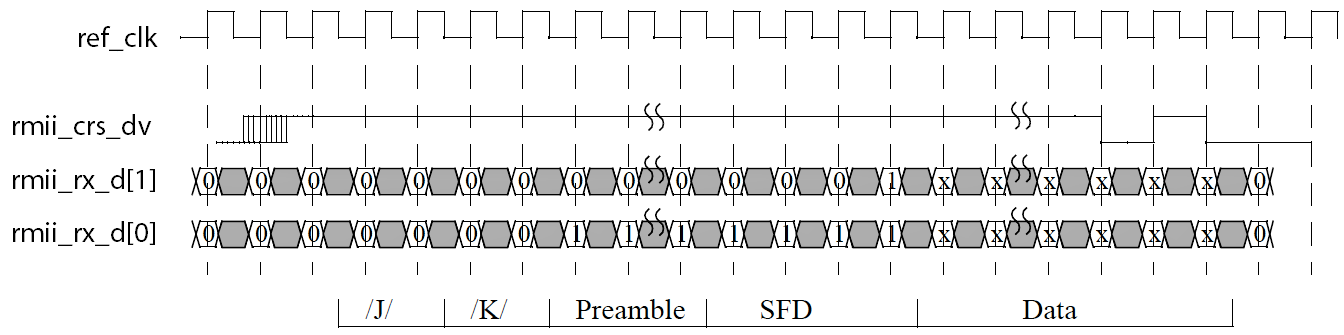
The PHY asserts the Carrier Sense or Receive Data Valid (rmii_crs_dv) signal when the receive medium is non-idle. The rmii_crs_dv is de-asserted synchronously if the carrier is lost, but only at nibble boundaries. If the PHY has additional bits to be presented on rmii_rx_d[1:0] following the loss of carrier, the PHY asserts the rmii_crs_dv on cycles of ref_clk which represent the second di-bit of each nibble.
At the nibble boundary, the rmii_crs_dv toggles at 25 MHz in 100 Mbps mode and 2.5 MHz in 10 Mbps mode on the event of carrier loss. This helps the IP core to recover the receive data valid and carrier sense signal.