1. FPGA AI Suite Design Examples User Guide
2. FPGA AI Suite Design Examples
3. Design Example Components
4. [PCIE] Getting Started with the FPGA AI Suite PCIe* -based Design Example
5. [PCIE] Building the FPGA AI Suite Runtime
6. [PCIE] Running the Design Example Demonstration Applications
7. [PCIE] Design Example System Architecture for the Agilex™ 7 FPGA
8. [OFS-PCIE] Getting Started with Open FPGA Stack (OFS) for PCIe* -Attach Design Examples
9. [OFS-PCIE] Design Example Components
10. [HL-NO-DDR] Getting Started with the FPGA AI Suite DDR-Free Design Example
11. [HL-NO-DDR] Running the Hostless DDR-Free Design Example
12. [HL-NO-DDR] Design Example System Architecture
13. [HL-NO-DDR] Quartus® Prime System Console
14. [HL-NO-DDR] JTAG to Avalon MM Host Register Map
15. [HL-NO-DDR] Updating MIF Files
16. [HL-JTAG] Getting Started
17. [HL-JTAG] Design Example Components
18. [SOC] FPGA AI Suite SoC Design Example Prerequisites
19. [SOC] FPGA AI Suite SoC Design Example Quick Start Tutorial
20. [SOC] FPGA AI Suite SoC Design Example Run Process
21. [SOC] FPGA AI Suite SoC Design Example Build Process
22. [SOC] FPGA AI Suite SoC Design Example Quartus® Prime System Architecture
23. [SOC] FPGA AI Suite SoC Design Example Software Components
24. [SOC] Streaming-to-Memory (S2M) Streaming Demonstration
A. FPGA AI Suite Example Designs User Guide Archives
B. FPGA AI Suite Example Designs User Guide Revision History
6.1. [PCIE] Exporting Trained Graphs from Source Frameworks
6.2. [PCIE] Compiling Exported Graphs Through the FPGA AI Suite
6.3. [PCIE] Compiling the PCIe* -based Example Design
6.4. [PCIE] Programming the FPGA Device ( Agilex™ 7)
6.5. [PCIE] Performing Accelerated Inference with the dla_benchmark Application
6.6. [PCIE] Running the Ported OpenVINO™ Demonstration Applications
8.2.1. [OFS-PCIE] Setup the OFS Environment for the FPGA Device
8.2.2. [OFS-PCIE] Exporting Trained Graphs from Source Frameworks.
8.2.3. [OFS-PCIE] Compiling Exported Graphs Through the FPGA AI Suite
8.2.4. [OFS-PCIE] Compiling the OFS for PCIe* Attach Design Example
8.2.5. [OFS-PCIE] Programming the FPGA Green Bitstream
8.2.6. [OFS-PCIE] Performing Accelerated Inference with the dla_benchmark application
16.1. [HL-JTAG] Prerequisites
16.2. [HL-JTAG] Building the FPGA AI Suite Runtime
16.3. [HL-JTAG] Building an FPGA Bitstream for the JTAG Design Examples
16.4. [HL-JTAG] Programming the FPGA Device
16.5. [HL-JTAG] Preparing Graphs for Inference with FPGA AI Suite
16.6. [HL-JTAG] Performing Inference on the Agilex™ 5 FPGA E-Series 065B Modular Development Kit
16.7. [HL-JTAG] Inference Performance Measurement
16.8. [HL-JTAG] Known Issues and Limitations
19.1. [SOC] Initial Setup
19.2. [SOC] Initializing a Work Directory
19.3. [SOC] (Optional) Create an SD Card Image (.wic)
19.4. [SOC] Writing the SD Card Image (.wic) to an SD Card
19.5. [SOC] Preparing SoC FPGA Development Kits for the FPGA AI Suite SoC Design Example
19.6. [SOC] Adding Compiled Graphs (AOT files) to the SD Card
19.7. [SOC] Verifying FPGA Device Drivers
19.8. [SOC] Running the Demonstration Applications
19.5.1. [SOC] Preparing the Agilex™ 5 FPGA E-Series 065B Modular Development Kit
19.5.2. [SOC] Preparing the Agilex™ 7 FPGA I-Series Transceiver-SoC Development Kit
19.5.3. [SOC] Preparing the Arria® 10 SX SoC FPGA Development Kit
19.5.4. [SOC] Configuring the SoC FPGA Development Kit UART Connection
19.5.5. [SOC] Determining the SoC FPGA Development Kit IP Address
19.5.1.1. [SOC] Confirming the Agilex™ 5 FPGA E-Series 065B Modular Development Kit Board Setup
19.5.1.2. [SOC] Programming the Agilex™ 5 FPGA Device with the JTAG Indirect Configuration (.jic) File
19.5.1.3. [SOC] Programming the Agilex™ 5 FPGA Device with the SRAM Object File (.sof)
19.5.1.4. [SOC] Connecting the Agilex™ 5 FPGA E-Series 065B Modular Development Kit to the Host Development System
19.5.2.1. [SOC] Confirming Agilex™ 7 FPGA I-Series Transceiver-SoC Development Kit Board Set Up
19.5.2.2. [SOC] Programming the Agilex™ 7 FPGA Device with the JTAG Indirect Configuration (.jic) File
19.5.2.3. [SOC] Programming the Agilex™ 7 FPGA Device with the SRAM Object File (.sof)
19.5.2.4. [SOC] Connecting the Agilex™ 7 FPGA I-Series Transceiver-SoC Development Kit to the Host Development System
22.1. [SOC] FPGA AI Suite SoC Design Example Inference Sequence Overview
22.2. [SOC] Memory-to-Memory (M2M) Variant Design
22.3. [SOC] Streaming-to-Memory (S2M) Variant Design
22.4. [SOC] Top Level
22.5. [SOC] The SoC Design Example Platform Designer System
22.6. [SOC] Fabric EMIF Design Component
22.7. [SOC] PLL Configuration
23.1.1. [SOC] Yocto Recipe: recipes-core/images/coredla-image.bb
23.1.2. [SOC] Yocto Recipe: recipes-bsp/u-boot/u-boot-socfpga_%.bbappend
23.1.3. [SOC] Yocto Recipe: recipes-drivers/msgdma-userio/msgdma-userio.bb
23.1.4. [SOC] Yocto Recipe: recipes-drivers/uio-devices/uio-devices.bb
23.1.5. [SOC] Yocto Recipe: recipes-kernel/linux/linux-socfpga-lts_%.bbappend
23.1.6. [SOC] Yocto Recipe: recipes-support/devmem2/devmem2_2.0.bb
23.1.7. [SOC] Yocto Recipe: wic
22.4. [SOC] Top Level
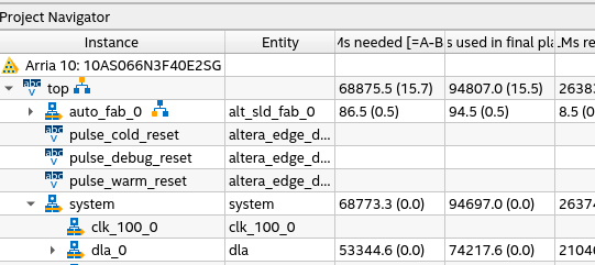
After the Quartus® Prime project has finished compiling, the design should look similar to the following image in the Quartus® Prime Project Navigator:
Figure 22. SoC Design Example Hierarchy
The top-level Verilog file and HPS configuration is derived directly from the GSRD designs located at the Altera FPGA Developer Site (https://altera-fpga.github.io) or RocketBoards.org:
- For more information about the GSRD for the Agilex™ 5 FPGA E-Series 065B Modular Development Kit, refer to the following URL: https://altera-fpga.github.io/latest/embedded-designs/agilex-5/e-series/modular/gsrd/ug-gsrd-agx5e-modular/.
- For more information about the GSRD for the Agilex™ 7 FPGA I-Series Transceiver-SoC Development Kit, refer to the following URL: https://altera-fpga.github.io/latest/embedded-designs/agilex-7/i-series/soc/gsrd/ug-gsrd-agx7i-soc/.
- For more information about the GSRD for the Arria® 10 SX SoC FPGA Development Kit, refer to the following URL: https://www.rocketboards.org/foswiki/Documentation/arria10SoCGSRD.
The GSRD designs have been modified to include the FPGA AI Suite IP. All unnecessary logic has been removed, which provides a concise design example.
The main FPGA AI Suite SoC design example is contained within a single Platform Designer system, called system. Double-click this node in the Quartus® Prime Project Navigator to launch Platform Designer.