9.1. [OFS-PCIE] Hardware Components
The FPGA AI Suite OFS for PCIe* attach design example is based on OFS (Open FPGA Stack). The following diagram shows a high-level view of a typical OFS system/A software stack runs on the host CPU (applications, OFS libraries, FPGA drivers) that connects via a PCIe connection to an FPGA board.
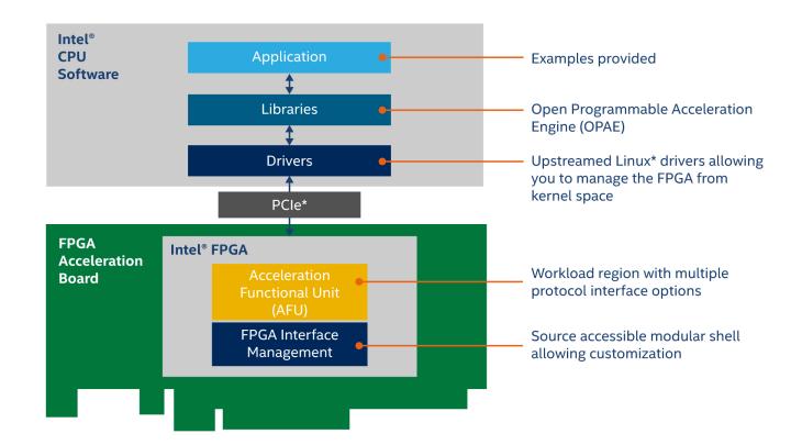
The design example hardware implementation, sits in the AFU (acceleration functional unit) region and uses the OFS FIM (FPGA interface manager) to connect to both the host CPU via a PCIe connection and also to the on-board DDR4 memory.
For more information about OFS, refer to the Open FPGA Stack (OFS) documentation.
The Agilex™ 7 FPGA I-Series Development Kit has four banks of DDR4 memory on board: two banks are soldered-on 8 GB of DDR4 memory each, two banks are DIMM slots for DDR4 DIMMs. For the design example, the DIMMs must also be 8GB in size each to match the soldered DDR4 memories. Larger size memories are currently not supported.
The Intel® FPGA SmartNIC N6001-PL Platform has four banks of DD4 memory on board. All banks are soldered-on 4 GB DDR4 DIMMs.
- Towards the host CPU via the PCIe connection two interfaces are exposed:
- A high-throughput AXI4 agent that initiates reads and writes from the FPGA fabric over the PCIe connection to the host CPU memory that is used by the DMA controller.
- An AXI4-Lite host so that initiates reads and writes from the host CPU to the FPGA fabric. This interface is used, mainly for configuring the FPGA AI Suite IP CSRs, the DMA CSR, and unaligned MMIO accesses of the FPGA DDRs.
- Towards the on-board FPGA DDR banks.
Four AXI4 agents, each of which connects to one DDR memory bank, connect to arbitration logic to enable the following paths into the DDR memory banks:
- DMA controller to DDR
- MIMO to DDR
- FPGA AI Suite IP to DDR.
- PCIe core clock (500 MHz)
- DDR core clock (333 MHz)
- User clock (configurable, typically around 600 MHz)
At the entry from the PCIe interface to the AFU, there are clock crossers from the PCIe core clock into the DDR core clock. The DDR core clock is used in all the DMA, CSR and arbitration logic to help benefit timing closure, while always still maintaining the full bandwidth to all four FPGA DDR banks.
The FPGA AI Suite IP runs on a configurable user clock and is set accordingly after the Quartus compile to match the maximum supported frequency of the IP in its chosen configuration. Typically, this frequency is 600 MHz and above for designs with only one FPGA AI Suite IP instance and just below 600 MHz for four FPGA AI Suite IP instances.
If the card shuts down in this way, the host machine issues a kernel panic (in Linux) and either freezes or reboots automatically.
If this occurs, you must reduce the target frequency of the FPGA AI Suite IP or reduce the number of FPGA AI Suite IP instances in your instantiation of the design example.