Intel Agilex® 7 F-Series and I-Series FPGA Memory Subsystem IP User Guide
ID
789389
Date
10/02/2023
Public
A newer version of this document is available. Customers should click here to go to the newest version.
1. About the Intel Agilex® 7 F-Series and I-Series FPGA Memory Subsystem IP
2. Introduction to Memory Subsystem IP
3. Memory Subsystem IP Architecture and Feature Description
4. Memory Subsystem Features
5. Memory Subsystem Interfaces and Signals
6. Memory Subsystem User Operations
7. Memory Subsystem Register Descriptions
8. Parameterizing the Memory Subsystem IP
9. Simulating Your Design
10. Document Revision History for Intel Agilex® 7 F-Series and I-Series FPGA Memory Subsystem IP User Guide
5.3.1. TCAM AXI-ST Request Interface
5.3.2. TCAM AXI-ST Response Interface
5.3.3. TCAM AXI-Lite Interface
5.3.4. BCAM AXI-ST Request Interface
5.3.5. BCAM AXI-ST Response Interface
5.3.6. BCAM AXI-Lite Interface
5.3.7. MBL AXI-ST Request Interface
5.3.8. MBL AXI-ST Response Interface
5.3.9. MBL AXI-Lite Interface
6.4.1. MBL Flush Operation
6.4.2. MBL Insert Key Operation
6.4.3. MBL Delete Key Operation
6.4.4. MBL Lookup Operation Using Key
6.4.5. MBL Modify Operation
6.4.6. MBL Modify Result Using Handle Operation
6.4.7. MBL Delete Key Using Handle Operation
6.4.8. MBL Lookup Using Handle Operation
6.4.9. MBL Insert Key if Not Present or Modify Result if Present Operation
6.4.10. MBL Get Handle Operation
7.2.1. Offset 0x0000 Version
7.2.2. Offset 0x0004 Feature List
7.2.3. Offset 0x0010h Interface Attribute Parameters
7.2.4. Offset 0x0020 Scratch Pad
7.2.5. Offset 0x0050 Status
7.2.6. Offset 0x0 0100 - 0x0 0xxx (+0x8h per instance), Additional Attributes Per Instance Lower DW (1 to 16)
7.2.7. Offset 0x0 0104 - 0x0 0xxx (+0x8h per instance) Additional Attributes per Instance Upper DW (1 up to 16)
7.2.8. Offset 0x0 1000 (+0x0 1000h per instance) Efficiency Monitor registers (per instance)
7.4.2.1. Version
7.4.2.2. Feature List
7.4.2.3. Interface Attribute Parameters
7.4.2.4. Interface Attribute Parameters 1
7.4.2.5. Scratch Pad
7.4.2.6. General Control (GEN_CTRL)
7.4.2.7. Management Control (MGMT_CTRL)
7.4.2.8. Hash function_0 seed
7.4.2.9. Hash function_1 seed
7.4.2.10. Hash function_2 seed
7.4.2.11. Warning 0 (WARNING_0)
7.4.2.12. Fatal Error (FATAL_ERROR_0)
7.4.2.13. Monitor 0 (MON_)
7.4.2.14. Total Entries (TOTAL_ENTRIES)
7.4.2.15. Max. Rehouse Iterations (Max_Rehouse_Iterations)
7.4.2.16. Statistics Control (STATS_CTRL)
7.4.2.17. Active Table Entries (TABLE_ENTRIES)
7.4.2.18. Key_N
7.4.2.19. Result_N
7.6.1. General MBL Registers
7.6.2. Version
7.6.3. Mbl_scratch
7.6.4. Mbl_gen_ctrl
7.6.5. Mbl_mgmt_ctrl
7.6.6. Mbl_key_handle
7.6.7. Mbl_nxt_handle_req
7.6.8. Mbl_nxt_handle
7.6.9. Mbl_warning_0
7.6.10. Mbl_fatal_0
7.6.11. Mbl_mon_0
7.6.12. Mbl_total_entries
7.6.13. Mbl_total_rehashes
7.6.14. Mbl_max_used_bins
7.6.15. Mbl_stats_ctrl
7.6.16. Mbl_stats_result
7.6.17. Mbl_max_lkup_latency
7.6.18. Mbl_max_rehash_index
7.6.19. Mbl_key
7.6.20. Mbl_res
8.2.5.1. Parameterizing the External Memory Interface (EMIF) IP
8.2.5.2. Parameterizing the Memory-Specific Adapter
8.2.5.3. Parameterizing the Content-Addressable Memory (CAM) IP
8.2.5.4. Parameterizing the External Memory Interfaces Intel Calibration IP
8.2.5.5. Saving the IPs Within the Memory Subsystem
8.2.5.6. Propagation of Changes Across IPs within the Memory Subsystem IP
8.2.5. Parameterizing Required EMIF, CAM, and MSA IPs
After you have configured the high-level topology, you can continue the parametrization ofl the sub-IPs within the memory subsystem.
The sub-IPs within the memory subsystem are as follows:
- External memory interface (EMIF) IP
- MSA IP
- EMIF for HPS IP
- CAM IPs (BCAM, TCAM, MBL)
To parameterize the sub-IPs, proceed as follows:
- Check the Generate IPs within Memory Subsystem checkbox.
- Click Dive Into Packaged Subsystem. A new Platform Designer window appears, listing the necessary controls to allow you to parametrize and fine-tune all the IPs that are part of the Memory Subsystem IP.
- Use the Platform Designer window to parameterize the individual IPs. Refer to the following topics for details.
The following figure depicts the Platform Designer window:
Figure 53. Example of the Platform Designer Window to Parametrize the Memory Subsystem IP
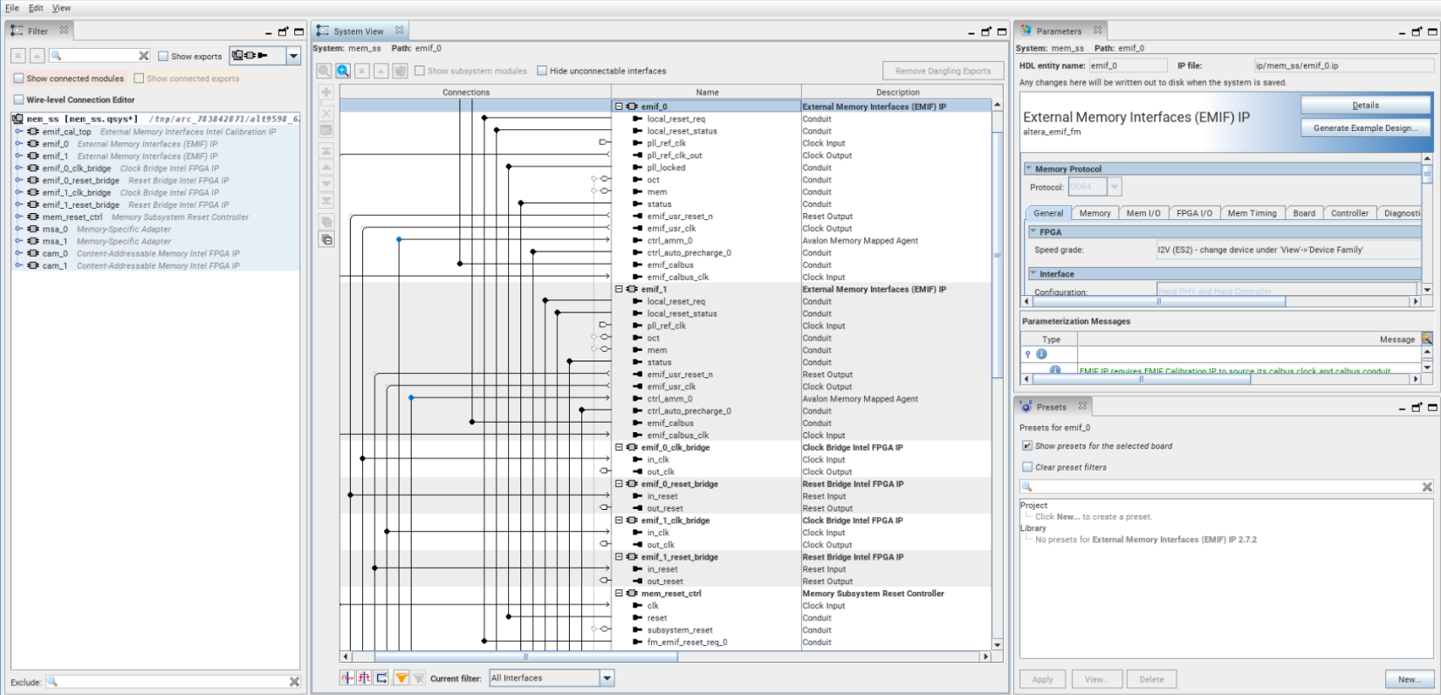
The Filter tab provides a quick overview of all instantiated IPs that are part of your memory subsystem IP. This figure is a continuation of the example discussed in the previous topics, and shows the expected IPs: one calibration IP for both EMIF IPs, their two associated MSA IPs, and two CAM IPs.
The following table shows how the configured high-level topology is translated to all the listed IPs:
| High-Level Topology | Associated IPs | ||
|---|---|---|---|
| Memory Interface | Application Interface | Main IPs | Calibration, Reset, and Bridge IPs |
| External: DDR4 | Storage | emif_0, msa_0 | emif_cal_top, emif_0_clk_bridge, emif_0_reset_bridge, mem_reset_ctrl |
| On-chip: M20K | Associative storage | cam_0 | |
| External: DDR4 | Associative storage | emif_1, msa_1, cam_1 | emif_cal_top, emif_1_clk_bridge, emif_1_reset_bridge, mem_reset_ctrl |
Section Content
Parameterizing the External Memory Interface (EMIF) IP
Parameterizing the Memory-Specific Adapter
Parameterizing the Content-Addressable Memory (CAM) IP
Parameterizing the External Memory Interfaces Intel Calibration IP
Saving the IPs Within the Memory Subsystem
Propagation of Changes Across IPs within the Memory Subsystem IP