Intel Agilex® 7 F-Series and I-Series FPGA Memory Subsystem IP User Guide
ID
789389
Date
10/02/2023
Public
A newer version of this document is available. Customers should click here to go to the newest version.
1. About the Intel Agilex® 7 F-Series and I-Series FPGA Memory Subsystem IP
2. Introduction to Memory Subsystem IP
3. Memory Subsystem IP Architecture and Feature Description
4. Memory Subsystem Features
5. Memory Subsystem Interfaces and Signals
6. Memory Subsystem User Operations
7. Memory Subsystem Register Descriptions
8. Parameterizing the Memory Subsystem IP
9. Simulating Your Design
10. Document Revision History for Intel Agilex® 7 F-Series and I-Series FPGA Memory Subsystem IP User Guide
5.3.1. TCAM AXI-ST Request Interface
5.3.2. TCAM AXI-ST Response Interface
5.3.3. TCAM AXI-Lite Interface
5.3.4. BCAM AXI-ST Request Interface
5.3.5. BCAM AXI-ST Response Interface
5.3.6. BCAM AXI-Lite Interface
5.3.7. MBL AXI-ST Request Interface
5.3.8. MBL AXI-ST Response Interface
5.3.9. MBL AXI-Lite Interface
6.4.1. MBL Flush Operation
6.4.2. MBL Insert Key Operation
6.4.3. MBL Delete Key Operation
6.4.4. MBL Lookup Operation Using Key
6.4.5. MBL Modify Operation
6.4.6. MBL Modify Result Using Handle Operation
6.4.7. MBL Delete Key Using Handle Operation
6.4.8. MBL Lookup Using Handle Operation
6.4.9. MBL Insert Key if Not Present or Modify Result if Present Operation
6.4.10. MBL Get Handle Operation
7.2.1. Offset 0x0000 Version
7.2.2. Offset 0x0004 Feature List
7.2.3. Offset 0x0010h Interface Attribute Parameters
7.2.4. Offset 0x0020 Scratch Pad
7.2.5. Offset 0x0050 Status
7.2.6. Offset 0x0 0100 - 0x0 0xxx (+0x8h per instance), Additional Attributes Per Instance Lower DW (1 to 16)
7.2.7. Offset 0x0 0104 - 0x0 0xxx (+0x8h per instance) Additional Attributes per Instance Upper DW (1 up to 16)
7.2.8. Offset 0x0 1000 (+0x0 1000h per instance) Efficiency Monitor registers (per instance)
7.4.2.1. Version
7.4.2.2. Feature List
7.4.2.3. Interface Attribute Parameters
7.4.2.4. Interface Attribute Parameters 1
7.4.2.5. Scratch Pad
7.4.2.6. General Control (GEN_CTRL)
7.4.2.7. Management Control (MGMT_CTRL)
7.4.2.8. Hash function_0 seed
7.4.2.9. Hash function_1 seed
7.4.2.10. Hash function_2 seed
7.4.2.11. Warning 0 (WARNING_0)
7.4.2.12. Fatal Error (FATAL_ERROR_0)
7.4.2.13. Monitor 0 (MON_)
7.4.2.14. Total Entries (TOTAL_ENTRIES)
7.4.2.15. Max. Rehouse Iterations (Max_Rehouse_Iterations)
7.4.2.16. Statistics Control (STATS_CTRL)
7.4.2.17. Active Table Entries (TABLE_ENTRIES)
7.4.2.18. Key_N
7.4.2.19. Result_N
7.6.1. General MBL Registers
7.6.2. Version
7.6.3. Mbl_scratch
7.6.4. Mbl_gen_ctrl
7.6.5. Mbl_mgmt_ctrl
7.6.6. Mbl_key_handle
7.6.7. Mbl_nxt_handle_req
7.6.8. Mbl_nxt_handle
7.6.9. Mbl_warning_0
7.6.10. Mbl_fatal_0
7.6.11. Mbl_mon_0
7.6.12. Mbl_total_entries
7.6.13. Mbl_total_rehashes
7.6.14. Mbl_max_used_bins
7.6.15. Mbl_stats_ctrl
7.6.16. Mbl_stats_result
7.6.17. Mbl_max_lkup_latency
7.6.18. Mbl_max_rehash_index
7.6.19. Mbl_key
7.6.20. Mbl_res
8.2.5.1. Parameterizing the External Memory Interface (EMIF) IP
8.2.5.2. Parameterizing the Memory-Specific Adapter
8.2.5.3. Parameterizing the Content-Addressable Memory (CAM) IP
8.2.5.4. Parameterizing the External Memory Interfaces Intel Calibration IP
8.2.5.5. Saving the IPs Within the Memory Subsystem
8.2.5.6. Propagation of Changes Across IPs within the Memory Subsystem IP
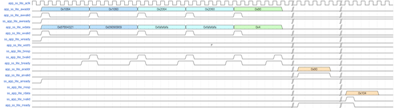
6.4.5. MBL Modify Operation
To perform a modify result using key operation, follow these steps through AXI Lite interface:
- Write the key to the MBL_KEY registers.
- Write the result to the MBL_RES registers.
- Poll the MBL_MGMT_CTRL register until the busy bit = 0x0.
- Write to the MBL_MGMT_CTRL register:
- Specifying req_type = 0x4.
- Specifying tab (logical table).
- Check MBL_MGMT_CTRL register success bit, success bit is set to 0x1 to indicate that the modify operation is handled successfully.
- The MBL_KEY_HANDLE register is written with a handle value corresponding to the key.
The following diagram shows a modify operation on MBL where:
- The address of mgmt_ctrl register is 0xb0, due to CSR_BASEADDR + CSR_ADDROFF + offset -> 0 + 0x60 + 0x20 = 0x80.
- The address of key_n register is 0x1060, due to CSR_BASEADDR + CSR_ADDROFF + offset -> 0 + 0x60 + 0x1000 = 0x1060.
- The address of result_n register is 0x2060, due to CSR_BASEADDR + CSR_ADDROFF + offset -> 0 + 0x60 + 0x2000 = 0x2060.
Figure 37. Modify Result Operation on MBL