External Memory Interfaces Intel Agilex® 7 M-Series FPGA IP User Guide
ID
772538
Date
4/03/2023
Public
A newer version of this document is available. Customers should click here to go to the newest version.
1. About the External Memory Interfaces Intel Agilex® 7 M-Series FPGA IP
2. Intel Agilex® 7 M-Series FPGA EMIF IP – Introduction
3. Intel Agilex® 7 M-Series FPGA EMIF IP – Product Architecture
4. Intel Agilex® 7 M-Series FPGA EMIF IP – End-User Signals
5. Intel Agilex® 7 M-Series FPGA EMIF IP – Simulating Memory IP
6. Intel Agilex 7 M-Series FPGA EMIF IP – DDR4 Support
7. Intel Agilex® 7 M-Series FPGA EMIF IP – DDR5 Support
8. Intel Agilex 7 M-Series FPGA EMIF IP – LPDDR5 Support
9. Intel Agilex® 7 M-Series FPGA EMIF IP – Timing Closure
10. Intel Agilex® 7 M-Series FPGA EMIF IP – Controller Optimization
11. Intel Agilex® 7 M-Series FPGA EMIF IP – Debugging
12. Document Revision History for External Memory Interfaces Intel Agilex® 7 M-Series FPGA IP User Guide
3.1.1. Intel Agilex® 7 M-Series EMIF Architecture: I/O Subsystem
3.1.2. Intel Agilex® 7 M-Series EMIF Architecture: I/O SSM
3.1.3. Intel Agilex® 7 M-Series EMIF Architecture: I/O Bank
3.1.4. Intel Agilex® 7 M-Series EMIF Architecture: I/O Lane
3.1.5. Intel Agilex® 7 M-Series EMIF Architecture: Input DQS Clock Tree
3.1.6. Intel Agilex® 7 M-Series EMIF Architecture: PHY Clock Tree
3.1.7. Intel Agilex® 7 M-Series EMIF Architecture: PLL Reference Clock Networks
3.1.8. Intel Agilex® 7 M-Series EMIF Architecture: Clock Phase Alignment
6.2.4.1. Address and Command Pin Placement for DDR4
6.2.4.2. DDR4 Data Width Mapping
6.2.4.3. General Guidelines
6.2.4.4. x4 DIMM Implementation
6.2.4.5. Specific Pin Connection Requirements
6.2.4.6. Command and Address Signals
6.2.4.7. Clock Signals
6.2.4.8. Data, Data Strobes, DM/DBI, and Optional ECC Signals
6.3.5.1. Single Rank x 8 Discrete (Component) Topology
6.3.5.2. Single Rank x 16 Discrete (Component) Topology
6.3.5.3. ADDR/CMD Reference Voltage/RESET Signal Routing Guidelines for Single Rank x 8 and Single Rank x 16 Discrete (Component) Topologies
6.3.5.4. Skew Matching Guidelines for DDR4 Discrete Configurations
6.3.5.5. Power Delivery Recommendations for DDR4 Discrete Configurations
6.3.5.6. Intel Agilex® 7 M-Series EMIF Pin Swapping Guidelines
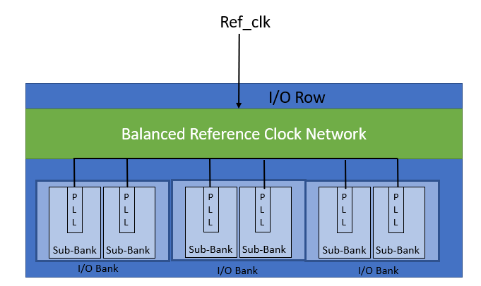
3.1.7. Intel Agilex® 7 M-Series EMIF Architecture: PLL Reference Clock Networks
Each sub-bank includes an I/O bank I/O PLL that can drive the PHY clock trees of that bank, through dedicated connections. In addition to supporting EMIF-specific functions, the I/O bank I/O PLLs can also serve as general-purpose PLLs for user logic.
The PLL reference clock must be constrained to the address and command sub-bank only.
Intel Agilex® 7 M-Series external memory interfaces that span multiple banks use the PLL in each bank. The Intel Agilex® 7 M-Series architecture allows for relatively short PHY clock networks, reducing jitter and duty-cycle distortion.
The following mechanisms ensure that the clock outputs of individual I/O bank I/O PLLs in a multi-bank interface remain in phase:
- A single PLL reference clock source feeds all I/O bank I/O PLLs. The reference clock signal reaches the PLLs by a balanced PLL reference clock tree. The Intel® Quartus® Prime software automatically configures the PLL reference clock tree so that it spans the correct number of banks. This clock must be free-running and stable prior to FPGA configuration.
- The EMIF IP sets the PLL configuration (counter settings, bandwidth settings, compensation and feedback mode setting) values appropriately to maintain synchronization among the clock dividers across the PLLs. This requirement restricts the legal PLL reference clock frequencies for a given memory interface frequency and clock rate. If you plan to use an on-board oscillator, you must ensure that its frequency matches the PLL reference clock frequency that you select from the displayed list.
Figure 7. PLL Balanced Reference Clock Tree