External Memory Interfaces Intel Agilex® 7 M-Series FPGA IP User Guide
ID
772538
Date
4/03/2023
Public
A newer version of this document is available. Customers should click here to go to the newest version.
1. About the External Memory Interfaces Intel Agilex® 7 M-Series FPGA IP
2. Intel Agilex® 7 M-Series FPGA EMIF IP – Introduction
3. Intel Agilex® 7 M-Series FPGA EMIF IP – Product Architecture
4. Intel Agilex® 7 M-Series FPGA EMIF IP – End-User Signals
5. Intel Agilex® 7 M-Series FPGA EMIF IP – Simulating Memory IP
6. Intel Agilex 7 M-Series FPGA EMIF IP – DDR4 Support
7. Intel Agilex® 7 M-Series FPGA EMIF IP – DDR5 Support
8. Intel Agilex 7 M-Series FPGA EMIF IP – LPDDR5 Support
9. Intel Agilex® 7 M-Series FPGA EMIF IP – Timing Closure
10. Intel Agilex® 7 M-Series FPGA EMIF IP – Controller Optimization
11. Intel Agilex® 7 M-Series FPGA EMIF IP – Debugging
12. Document Revision History for External Memory Interfaces Intel Agilex® 7 M-Series FPGA IP User Guide
3.1.1. Intel Agilex® 7 M-Series EMIF Architecture: I/O Subsystem
3.1.2. Intel Agilex® 7 M-Series EMIF Architecture: I/O SSM
3.1.3. Intel Agilex® 7 M-Series EMIF Architecture: I/O Bank
3.1.4. Intel Agilex® 7 M-Series EMIF Architecture: I/O Lane
3.1.5. Intel Agilex® 7 M-Series EMIF Architecture: Input DQS Clock Tree
3.1.6. Intel Agilex® 7 M-Series EMIF Architecture: PHY Clock Tree
3.1.7. Intel Agilex® 7 M-Series EMIF Architecture: PLL Reference Clock Networks
3.1.8. Intel Agilex® 7 M-Series EMIF Architecture: Clock Phase Alignment
6.2.4.1. Address and Command Pin Placement for DDR4
6.2.4.2. DDR4 Data Width Mapping
6.2.4.3. General Guidelines
6.2.4.4. x4 DIMM Implementation
6.2.4.5. Specific Pin Connection Requirements
6.2.4.6. Command and Address Signals
6.2.4.7. Clock Signals
6.2.4.8. Data, Data Strobes, DM/DBI, and Optional ECC Signals
6.3.5.1. Single Rank x 8 Discrete (Component) Topology
6.3.5.2. Single Rank x 16 Discrete (Component) Topology
6.3.5.3. ADDR/CMD Reference Voltage/RESET Signal Routing Guidelines for Single Rank x 8 and Single Rank x 16 Discrete (Component) Topologies
6.3.5.4. Skew Matching Guidelines for DDR4 Discrete Configurations
6.3.5.5. Power Delivery Recommendations for DDR4 Discrete Configurations
6.3.5.6. Intel Agilex® 7 M-Series EMIF Pin Swapping Guidelines
3.1.8. Intel Agilex® 7 M-Series EMIF Architecture: Clock Phase Alignment
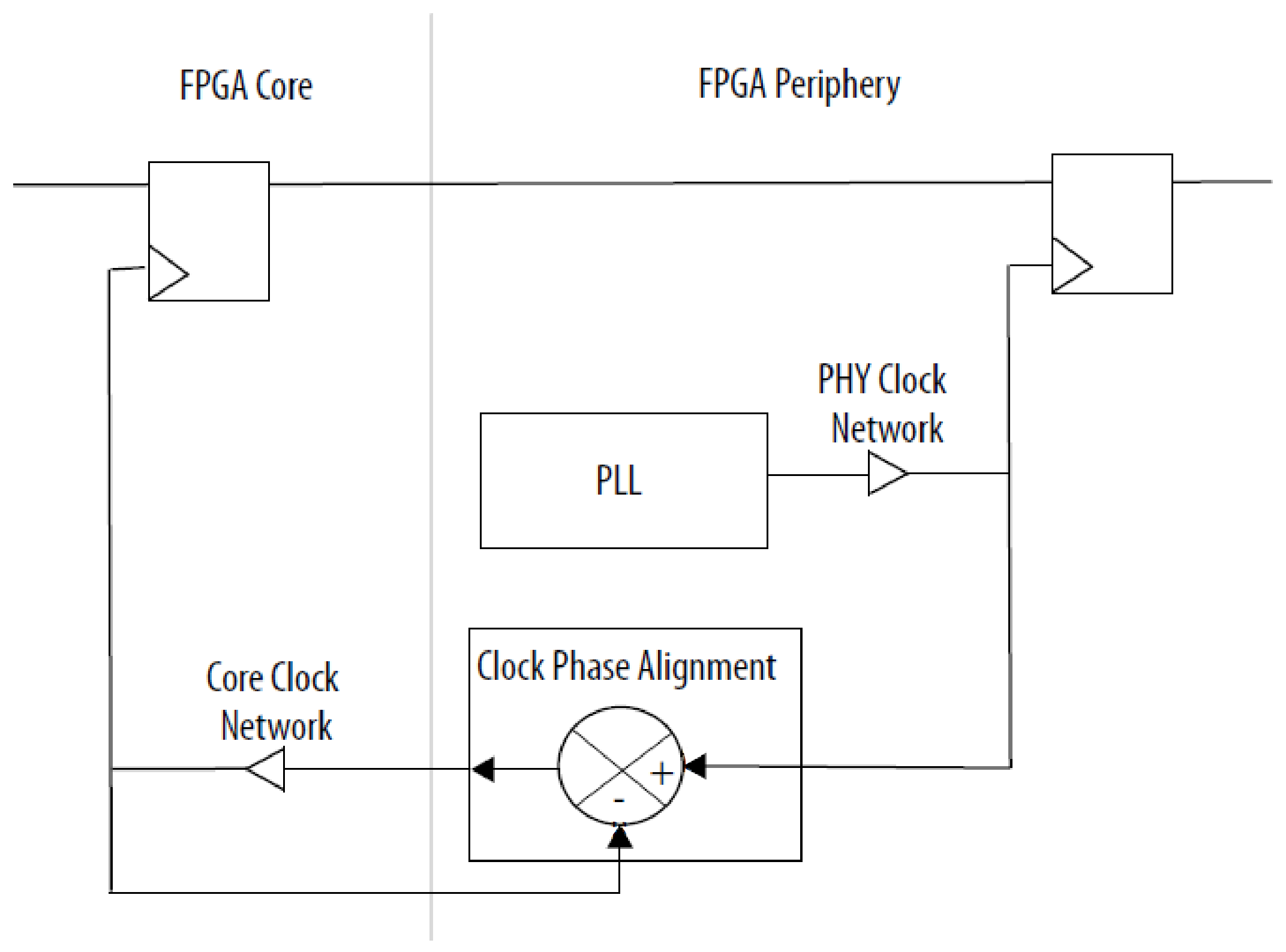
In Intel Agilex® 7 M-Series external memory interfaces, a global clock network clocks registers inside the FPGA core, and the PHY clock network clocks registers inside the FPGA periphery. Clock phase alignment circuitry employs negative feedback to dynamically adjust the phase of the core clock signal to match the phase of the PHY clock signal.
The clock phase alignment feature effectively eliminates the clock skew effect in all transfers between the core and the periphery, facilitating timing closure. All Intel Agilex® 7 M-Series external memory interfaces employ clock phase alignment circuitry.
Figure 8. Clock Phase Alignment Illustration


Figure 9. Effect of Clock Phase Alignment

