Embedded Peripherals IP User Guide

ID 683130
Date 2/09/2023
Public

A newer version of this document is available. Customers should click here to go to the newest version.

Document Table of Contents
1. Introduction 2. Avalon® -ST Multi-Channel Shared Memory FIFO Core 3. Avalon® -ST Single-Clock and Dual-Clock FIFO Cores 4. Avalon® -ST Serial Peripheral Interface Core 5. SPI Core 6. SPI Agent/JTAG to Avalon® Host Bridge Cores 7. Intel eSPI Agent Core 8. eSPI to LPC Bridge Core 9. Ethernet MDIO Core 10. Intel FPGA 16550 Compatible UART Core 11. UART Core 12. JTAG UART Core 13. Intel FPGA Avalon® Mailbox Core 14. Intel FPGA Avalon® Mutex Core 15. Intel FPGA Avalon® I2C (Host) Core 16. Intel FPGA I2C Agent to Avalon® -MM Host Bridge Core 17. Intel FPGA Avalon® Compact Flash Core 18. EPCS/EPCQA Serial Flash Controller Core 19. Intel FPGA Serial Flash Controller Core 20. Intel FPGA Serial Flash Controller II Core 21. Intel FPGA Generic QUAD SPI Controller Core 22. Intel FPGA Generic QUAD SPI Controller II Core 23. Interval Timer Core 24. Intel FPGA Avalon FIFO Memory Core 25. On-Chip Memory (RAM and ROM) Intel FPGA IP 26. On-Chip Memory II (RAM or ROM) Intel FPGA IP 27. Optrex 16207 LCD Controller Core 28. PIO Core 29. PLL Cores 30. DMA Controller Core 31. Modular Scatter-Gather DMA Core 32. Scatter-Gather DMA Controller Core 33. SDRAM Controller Core 34. Tri-State SDRAM Core 35. Video Sync Generator and Pixel Converter Cores 36. Intel FPGA Interrupt Latency Counter Core 37. Performance Counter Unit Core 38. Vectored Interrupt Controller Core 39. Avalon® -ST Data Pattern Generator and Checker Cores 40. Avalon® -ST Test Pattern Generator and Checker Cores 41. System ID Peripheral Core 42. Avalon® Packets to Transactions Converter Core 43. Avalon® -ST Multiplexer and Demultiplexer Cores 44. Avalon® -ST Bytes to Packets and Packets to Bytes Converter Cores 45. Avalon® -ST Delay Core 46. Avalon® -ST Round Robin Scheduler Core 47. Avalon® -ST Splitter Core 48. Avalon® -MM DDR Memory Half Rate Bridge Core 49. Intel FPGA GMII to RGMII Converter Core 50. Intel FPGA MII to RMII Converter Core 51. Intel FPGA HPS GMII to TSE 1000BASE-X/SGMII PCS Bridge Core 52. Intel FPGA HPS EMAC to Multi-rate PHY GMII Adapter Core 53. Intel FPGA MSI to GIC Generator Core 54. Cache Coherency Translator Intel® FPGA IP 55. Lightweight UART Core

38.7.3. Software Description

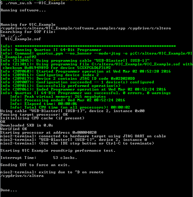
The software for the various example designs is very similar. For example, the difference between the software for the VIC Basic example and the software for the IIC example is the printf() call that generates the output to the terminal.

All of the software performs the following steps:

  1. Configures the timer used for measurement purposes
  2. Registers an interrupt service routine (ISR)
  3. Sets a global variable to 0xfeedface
  4. Starts the performance counter to measure the interrupt time
  5. Waits for the ISR to set the global variable to 0xfacefeed
  6. Stops the performance counter and computes the interrupt time

The VIC Daisy-Chain example performs the measurement for both VICs connected in the daisy chain, shown in Figure 141.

In all these design examples, the GCC compiler in Nios® II SBT tool is set to optimization level 2. Also, some settings are modified during BSP generation in order to reduce the code size. All these setting can be found in the create-this-bsp script included in the design example. Note that the number of clock cycles shows in these design examples will be differ from this document if the setting is different.

For details about how the VIC Table-Resident example code works, refer to “Positioning the ISR in the Vector Table”. For details about performance counter usage in the example software, refer to “Latency Measurement with the Performance Counter”.

VIC Example