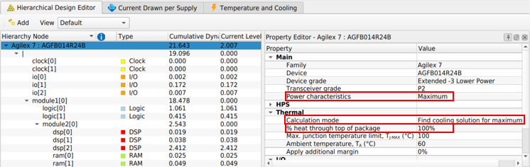
3.7. PTA - Temperature and Cooling Tab
| 4”x4” PCB with 2s2p | 10”x10” PCB with 10 layers | ||||||||
|---|---|---|---|---|---|---|---|---|---|
| Airflow (lfm) | 0 | 100 | 200 | 400 | 0 | 100 | 200 | 400- | |
| No Heatsink | 10% | 15% | 20% | 25% | 10% | 15% | 20% | 25% | |
| 25mm x 25mm x 5mm Heatsink | 15% | 30% | 40% | 50% | 10% | 20% | 30% | 40% | |
| 30mm x 30mm x 15mm Heatsink | 40% | 70% | 80% | 80% | 30% | 60% | 70% | 80% | |
| 50mm x 50mm x 25mm Heatsink | 70% | 80% | 85% | 90% | 55% | 75% | 80% | 80% | |
| Column Heading | Description |
|---|---|
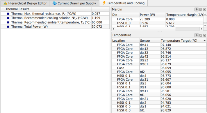
| Thermal Max. thermal resistance, ΨJC(⁰C/W) | ΨJC is the thermal resistance between each of the dies in the package and the center of the package integrated heat spreader. This field shows the maximum ΨJC among all dies, assuming the recommended ΨCA value below. |
| Thermal Recommended Cooling Solution ΨCA(⁰C/W) | ΨCA is the thermal resistance between the center of the package integrated heat spreader (IHS) and ambient temperature. The recommended ΨCA is the highest possible thermal resistance of the cooling solution that ensures no part of any die exceeds the specified maximum junction temperature. |
| Thermal Recommended Ambient Temperature, TA(⁰C) | TA is the recommended ambient temperature for the recommended cooling solution. |
| Total Power (W) | The total power consumption. |
| Thermal Die | The die for which margin is reported:
|
| Thermal Power (W) | The thermal power dissipated by the specified die. This is the power used in the thermal analysis.
Note: The power listed on the Thermal Margin Report is currently pessimistic; the overall total power reported does not match the total on-chip power dissipation on the Power Summary panel.
|
| Thermal Temperature Margin (delta ⁰C) | The calculated temperature margin in °C for the specified die, relative to the maximum TJ. |
| Thermal Power Margin (delta W) | The amount of power in watts that can be added to the specified die, before reaching its maximum TJ. |
Temperature margins are calculated relative to a designated maximum junction temperature, TJ. It is possible that one or more dies may have zero temperature margin, because the solution is calculated for that maximum TJ. The calculated power margins indicate the power margin available before the maximum TJ is exceeded, assuming the same cooling conditions. The calculated power value provides only an approximate estimate of power that can be added to the specific die before reaching its maximum TJ. The actual margin depends on the specific subsystem to which the power is added. Any increase or decrease in power changes the required cooling solution.
| Column Heading | Description |
|---|---|
| Thermal Location | The die for which the temperature is reported:
|
| Thermal Sensor | The digital thermal sensor (DTS) or thermal diode (TD) sensor reporting the temperature. |
| Thermal Temperature Target (⁰C) | The calculated temperature for the target location and sensor, when the system is operating. |
The monitor sensors report FPGA temperatures at the specified locations when the system is operating. These sensors may not necessarily be at the hottest locations on the die, and therefore can report values that are lower than the actual maximums in the design.
| Row Name | Description | |
|---|---|---|
| Total Power (W) | Provides total power consumption of all dies in the package. | |
| FPGA Core Power (W) | The total thermal power consumption of the main FPGA die containing core logic, assuming the recommended ΨCA value. This power is reported at the actual temperature of the core die, assuming the recommended ΨCA value. This temperature may be equal to the maximum junction temperature if the FPGA core die is at the highest temperature among all dies (also known as a hot spot). The FPGA core may also be at a lower temperature, if the hot spot is elsewhere in the package (i.e. on another die). | |
| Transceiver Thermal Power (W) | HSSI_0_0 | The total power consumption of HSSI_0_0, assuming the recommended ΨCA value. This power is reported at the actual temperature of the specific die, assuming the recommended ΨCA value above. This temperature may be equal to the maximum junction temperature if a specific die is the hot spot, or it may be at a lower temperature if the hot spot is elsewhere in the package.
Note: Each transceiver die in the package reports a small amount of static power even when no channels are used in the corresponding transceiver tile and transceiver rails (VCCR_GXB, VCCT_GXB, and VCCH_GXB) of that tile are grounded. This is an expected result.
|
| HSSI_1_0 | ||
| HSSI_2_0 | ||
| HSSI_0_1 | ||
| HSSI_1_1 | ||
| HSSI_2_1 | ||
| HBM Thermal Power (W) | HBM TOP | The total thermal power consumption of HBM TOP or HBM BOT, assuming the recommended ΨCA value. This power is reported at the actual temperature of the specific die, assuming the recommended ΨCA value above. This temperature may be equal to the maximum junction temperature if a specific die is the hot spot, or it may be at a lower temperature if the hot spot is elsewhere in the package. |
| HBM BOT | ||
| Row Name | Description | |
|---|---|---|
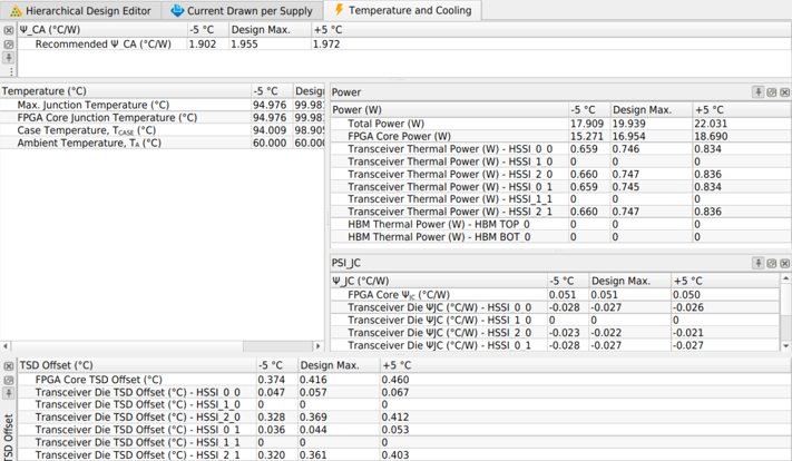
| Recommended ΨCA (°C/W) | The thermal resistance between the center of the package integrated heat spreader and the ambient temperature, assuming the specific core temperature in the given table row. For each row, this is the ΨCA value that would cause the FPGA core junction temperature to be at the specific value for a given row. | |
| Row Name | Description | |
|---|---|---|
| FPGA Core ΨJC(°C/W) | The thermal resistance between the main FPGA core die and the center of the package integrated heat spreader, assuming the recommended ΨCA value. | |
| Transceiver Die ΨJC(°C/W) | HSSI_0_0 | The thermal resistance between HSSI_0_0 and the center of the package integrated heat spreader, assuming the recommended ΨCA value. |
| HSSI_1_0 | ||
| HSSI_2_0 | ||
| HSSI_0_1 | ||
| HSSI_1_1 | ||
| HSSI_2_1 | ||
| HBM Die ΨJC(°C/W) | HBM TOP | The thermal resistance between HBM TOP or HBM BOT and the center of the package integrated heat spreader, assuming the recommended ΨCA value. |
| HBM BOT | ||
| Row Name | Description | |
|---|---|---|
| FPGA Core TSD Offset (°C) | The temperature difference between the hot spot on the main FPGA core and location of the thermal sensing diode (TSD) with the highest temperature reported using the Temperature IP Sense software. (When the IP sense method is used to read the TSDs, all the TSD locations are read and the highest of these is reported.) | |
| Transceiver Die TSD Offset (°C) | HSSI_0_0 | The temperature difference between the hot spot on the corresponding transceiver die and location of the thermal sensing diode (TSD) with the highest temperature reported using the Temperature IP Sense software. (When the IP sense method is used to read the TSDs, all the TSD locations are read and the highest of these is reported.) FPGA transceiver temperature = FPGA transceiver TSD temperature measured using the IP sense method + Transceiver TSD offset(If you are not using the Temperature IP Sense software to read the TSD offsets, contact your support representative for a workaround to get the correct TSD temperature.) |
| HSSI_1_0 | ||
| HSSI_2_0 | ||
| HSSI_0_1 | ||
| HSSI_1_1 | ||
| HSSI_2_1 | ||
For more information about HSSI_x_y locations, refer to the Physical Package Structure topic in AN 787: Stratix 10 Thermal Modeling and Management.
The tables above show variations of thermal parameters and power consumption with changing junction temperature of the main FPGA core die. Three values are provided for each parameter. The Design Max column contains FPGA core temperature and other parameters assuming the recommended ΨCA value above. The -5°C column provides values of all parameters when FPGA core temperature is 5°C lower than in the Design Max column. Similarly, the +5°C column provides values of all parameters when FPGA core temperature is 5°C higher than in the Design Max column. It is important to realize that under the conditions in the +5°C column at least one part of one die in the package exceeds the requested maximum junction temperature, and may even exceed the maximum allowed value for the device. Therefore the values in the +5°C column should be used only as an estimate of power dependence on temperature for the purpose of computational fluid dynamic (CFD) simulation, and not for any other purpose.
In extreme cases, such as thermal runaway, it may not be possible to calculate the values for +/- 5 degrees, in which case the Thermal worksheet displays the error message: ERROR: Could not calculate parameter variation with core temperature. Try adjusting TJ-MAX to obtain temperature-dependent parameters. When this error occurs, the recommended ΨCA value and all other values above are valid, but the table showing variation of thermal parameters and power consumption with changing junction temperature of the main FPGA core die contains some invalid values. As the error text indicates, adjusting the maximum junction temperature may allow the thermal solver to calculate this dependence, albeit at a different range of FPGA core temperatures than the usual range.