4.2. PTA - Root Entry
The required parameters depend on whether the junction temperature is manually entered or auto computed.
| Group | Parameter | Description |
|---|---|---|
| Transceiver | Treatment of unused transceivers | For Agilex™ FPGA portfolio device designs, specifies how unused transceivers, or used transceivers with unused channels, should be treated. The following options are available:
|
| Thermal | TSD Mode | Indicates the method by which sensor temperatures are reported. This parameter has no effect on maximum junction temperature or temperature margin. |
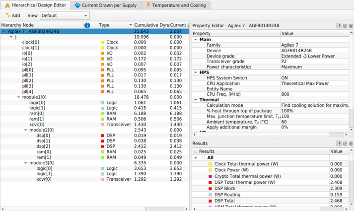
| Max Junction Temp, TJ-MAX (⁰C) | Allows you to specify the maximum junction temperature that no part of any die in the package should exceed. | |
| % Heat Through Top of Package | Specify the portion of heat that passes through the top of the package. | |
| Junction Temperature, TJ (⁰C) | Specify the junction temperature for all dies in the package. This field is available when you select Use a constant junction temperature as the Calculation mode. In this mode, the junction temperatures for all dies in the package are assumed to have the specified value. To automatically compute junction temperatures, select one of the other options in the same field. | |
| Cooling Solution ΨCA(⁰C/W) | Allows you to specify the cooling solution when you have selected the Use a constant junction temperature, Find available thermal margin for cooling solution, or Find ambient temperature for specified cooling solution calculation mode. | |
| Calculation Mode | Specifies the calculation mode for the thermal solver to use. The available choices are:
Note: To enable selection of non-constant calculation modes, the Power characteristics field in the Device selection group box must be set to Maximum.
|
|
| Apply Additional Margin | Specifies, as a percentage, the amount of additional margin to apply to detailed thermal analysis results. The default value is 0%. Valid values are 0-25%. The recommended margin for Agilex 5 and Agilex™ 7 devices is 10%. Consult your Field Application Engineer (FAE) if you require additional guidance on margin power. | |
| Ambient Temp, TA (⁰C) | Allows you to specify the temperature of the air that is cooling the device. | |
| Main | Transceiver grade | Select the required transceiver speed grade. |
| Power characteristics | Select typical or maximum power. There is a process variation from die-to-die. This variation primarily affects static power consumption. If you choose Typical power characteristics, estimates are based on long term projections of average power consumed by typical silicon. For FPGA board power supply design and thermal design, choose Maximum for worst-case values.
Note: Typical power characteristics should not be used for regulator sizing or thermal analysis; use Maximum power characteristics for these activities.
|
|
| Package | Select the device package. Larger packages provide a larger cooling surface and more contact points to the circuit board; thus they offer lower thermal resistance. Package selection does not affect dynamic power directly. | |
| Family | Shows the device family selected at startup, either directly or through the imported file. | |
| Device Grade | Select the combination of Operating Temperature, Speed Grade, and Power Option used. Refer to the device datasheet for available combinations. | |
| Device | Select your device. Larger devices consume more static power and have higher clock dynamic power. All other power components are unaffected by device selection. The parameter and value table on the right side of the PTA root entry displays specifications of the currently selected device. | |
| I/O | Voltage setting for unused HVIO banks | Select a value to calculate voltage of unused HVIO banks. This field applies only to Agilex 5 devices. Available values are 1.8V, 2.5V, 3.3V, and Power Down Unused GPIO Banks. |
| Voltage setting for unused GPIO banks | Select a value to calculate voltage of unused GPIO banks. Available values are 1.0V, 1.05V, 1.1V, 1.2V, 1.3V, 1.5V, and Power Down Unused GPIO Banks.
Note: The availability of some voltage settings depend on the device selected.
|
|
| HPS | VCCL HPS Voltage (mV) | Specifies the core HPS voltage (in mV). |
| Treatment of unused HPS cores | Set whether unused HPS cores shall be powered up. | |
| L3 Cache Size (MB) | Size of the L3 Cache. | |
| HPS System Switch | Turns the HPS system on or off. This selection affects the static power. | |
| Entity Name | Specify an entity name in this column. This is an optional value. | |
| CPU Freq. (MHz) | Specifies the operating frequency of all CPUs (in MHz). | |
| CPU Application | Select a benchmark application representative of the application running on the CPUs. | |
| A76 Cores | Number of A76 CPU Cores. | |
| A55 Cores | Number of A55 CPU Cores. | |
| A53 Cores | Number of A53 CPU Cores. |
| Group | Parameter | Description |
|---|---|---|
| Main | Device | The currently selected device. Larger devices consume more static power and have higher clock dynamic power. All other power components are unaffected by device selection. The parameter and value table on the right side of the PTA root entry displays specifications of the currently selected device. |
| Power Characteristics | Select typical or maximum power. There is a process variation from die-to-die. This variation primarily affects static power consumption. If you choose Typical power characteristics, estimates are based on long term projections of average power consumed by typical silicon. For FPGA board power supply design and thermal design, choose Maximum for worst-case values.
Note: Typical power characteristics should not be used for regulator sizing or thermal analysis; use Maximum power characteristics for these activities.
|
|
| Device Grade | Select the combination of Operating Temperature, Speed Grade, and Power Option used. Refer to the device datasheet for available combinations. | |
| Package | Select the device package. Larger packages provide a larger cooling surface and more contact points to the circuit board; thus they offer lower thermal resistance. Package selection does not affect dynamic power directly. | |
| Transceiver Grade | Select the required transceiver speed grade. | |
| VCC Voltage (mV) | VCC Rail Voltage (where applicable). | |
| Thermal | Calculation Mode | Specifies the calculation mode for the thermal solver to use. The available choices are these:
Note: To enable selection of non-constant calculation modes, the Power characteristics field in the Device selection group box must be set to Maximum.
|
| TSD Mode | Specify the method by which offset temperatures are provided—such as from a thermal diode, or a digital temperature sensing mechanism. | |
| Cooling Solution ΨCA(°C/W) | ψCA is the thermal resistance between the center of the package integrated heat spreader (IHS) and ambient temperature. The recommended ΨCA is the highest possible thermal resistance of the cooling solution that ensures no part of any die exceeds the specified maximum junction temperature. | |
| Apply Additional Margin | Specifies as a percentage, the amount of additional margin to apply to detailed thermal analysis results. The default value is 0%. Valid values are 0–25%. The recommended margin for Stratix 10 devices is 25%. Consult your Field Application Engineer (FAE) if you require additional guidance on margin power.
Note:
|
|
| Junction temperature, TJ (°C) | Specify the junction temperature for all dies in the package. This field applies only when the selected Calculation mode value is Use a constant junction temperature. | |
| Max. Junction Temp, TJ-MAX (°C) | Specify the maximum junction temperature that no part of any die in the package should exceed. | |
| Ambient Temp, TA (°C) | Specify the temperature of the air that is cooling the device. | |
| HPS | HPS System Switch | Turns the HPS system on or off. This selection affects the static power. |
| CPU Application | Select a benchmark application representative of the application running on the CPUs. | |
| VCCL_HPS Voltage (mV) | Specifies the core HPS voltage (in mV). | |
| Entity Name | Specifies a name for the entity. This is an optional value. | |
| CPU Freq. (MHz) | Specifies the operating frequency of all CPUs (in MHz). | |
| Number of CPU Cores | Specifies the number of cores in the CPU running the selected application. | |
| Transceiver | Treatment of unused transceiver dies | For Stratix® 10 devices, if you use no transceiver channels or PLLs on an HSSI die, you can power down the die or the die can remain powered. You can select the voltage of unused dies that are powered to minimize static power, or to minimize the number of power supply voltages required. For example, if active H-tile transceiver channels use VCCR_GXB=1.12V, selecting Minimize Leakage assumes that the unused-but-powered H-tile dies use VCCR_GXB=1.03V, which is the lowest supported voltage, thus minimizing leakage. Selecting Minimize Number of Supply Voltages assumes that the unused-but-powered banks use VCCR_GXB=1.12V, which is the voltage used by active channels, thus eliminating the need for the 1.03V power supply on VCCR_GXB. The PTA uses information in the XCVR Die ID, Starting Channel Location, and # of Channels properties on Transceiver resource entries, along with the # PLL Blocks and XCVR Die ID properties on PLL resource entries to determine whether dies are actively used. This setting does not apply to E-tile nor P-tile transceivers, because these transceiver dies can never be powered down. |