MIPI D-PHY IP User Guide: Agilex™ 3 and Agilex™ 5 FPGAs
ID
817561
Date
6/30/2025
Public
1. About the MIPI D-PHY IP
2. Configuring and Generating the MIPI D-PHY IP
3. MIPI D-PHY Interface Design Guidelines
4. Simulating the MIPI D-PHY IP
5. Validating the MIPI D-PHY IP
6. Debugging the MIPI-PHY IP
7. MIPI D-PHY Architecture
8. Interface Signals and Register Maps
9. Verification Test Plan
10. Document Revision History for the MIPI D-PHY IP User Guide
6.1. Creating a Simplified Design that Demonstrates the Same Problem
6.2. Evaluating FPGA Timing Problems
6.3. Determining if the Problem Exists in Previous Quartus Prime Versions
6.4. Determining if the Problem Exists in the Current Version of Software
6.5. Verifying the MIPI D-PHY IP Using the Signal Tap Logic Analyzer
6.6. Varying the Voltage
6.7. Operating at Lower Speed
6.8. Trying a Different PCB
8.2.1.1. IP_ID
8.2.1.2. IP_CAP
8.2.1.3. D0_CAP
8.2.1.4. DN_CAP
8.2.1.5. RX_CAP
8.2.1.6. TX_CAP
8.2.1.7. TX_PREAMBLE_LEN
8.2.1.8. D-PHY_CSR
8.2.1.9. TX_CLK_LANE_PS
8.2.1.10. RX_DLANE_ERR
8.2.1.11. SKEW_CAL_LEN_B0
8.2.1.12. SKEW_CAL_LEN_B1
8.2.1.13. SKEW_CAL_LEN_B2
8.2.1.14. SKEW_CAL_LEN_B3
8.2.1.15. ALT_CAL_LEN_B0
8.2.1.16. ALT_CAL_LEN_B1
8.2.1.17. ALT_CAL_LEN_B2
8.2.1.18. ALT_CAL_LEN_B3
8.2.1.19. CLK_CSR
8.2.1.20. CLK_STATUS
8.2.1.21. DLANE_CSR_0
8.2.1.22. DLANE_STATUS_0
8.2.1.23. RX_DLANE_DESKEW_DELAY_0
8.2.1.24. RX_DLANE_ERR_0
8.2.1.25. DLANE_CSR_1
8.2.1.26. DLANE_STATUS_1
8.2.1.27. RX_DLANE_DESKEW_DELAY_1
8.2.1.28. RX_DLANE_ERR_1
8.2.1.29. DLANE_CSR_2
8.2.1.30. DLANE_STATUS_2
8.2.1.31. RX_DLANE_DESKEW_DELAY_2
8.2.1.32. RX_DLANE_ERR_2
8.2.1.33. DLANE_CSR_3
8.2.1.34. DLANE_STATUS_3
8.2.1.35. RX_DLANE_DESKEW_DELAY_3
8.2.1.36. RX_DLANE_ERR_3
8.2.1.37. DLANE_CSR_4
8.2.1.38. DLANE_STATUS_4
8.2.1.39. RX_DLANE_DESKEW_DELAY_4
8.2.1.40. RX_DLANE_ERR_4
8.2.1.41. DLANE_CSR_5
8.2.1.42. DLANE_STATUS_5
8.2.1.43. RX_DLANE_DESKEW_DELAY_5
8.2.1.44. RX_DLANE_ERR_5
8.2.1.45. DLANE_CSR_6
8.2.1.46. DLANE_STATUS_6
8.2.1.47. RX_DLANE_DESKEW_DELAY_6
8.2.1.48. RX_DLANE_ERR_6
8.2.1.49. DLANE_CSR_7
8.2.1.50. DLANE_STATUS_7
8.2.1.51. RX_DLANE_DESKEW_DELAY_7
8.2.1.52. RX_DLANE_ERR_7
8.2.1.53. TX_LPX
8.2.1.54. TX_HS_EXIT
8.2.1.55. TX_LP_EXIT
8.2.1.56. TX_CLK_PREPARE
8.2.1.57. TX_CLK_ZERO
8.2.1.58. TX_CLK_POST
8.2.1.59. TX_CLK_PRE
8.2.1.60. TX_HS_PREPARE
8.2.1.61. TX_HS_ZERO
8.2.1.62. TX_HS_TRAIL
8.2.1.63. TX_INIT
8.2.1.64. TX_WAKE
8.2.1.65. RX_CLK_LOSS_DETECT
8.2.1.66. RX_CLK_SETTLE
8.2.1.67. RX_HS_SETTLE
8.2.1.68. RX_INIT
8.2.1.69. RX_CLK_POST
8.2.1.70. RX_CAL_REG_CTRL
8.2.1.71. RX_CAL_STATUS_D-PHY
8.2.1.72. RX_CAL_SKEW_W_START_MUX
8.2.1.73. RX_CAL_SKEW_W_END_MUX
8.2.1.74. RX_CAL_ALT_W_START_MUX
8.2.1.75. RX__CAL_ALT_W_END_MUX
8.2.1.76. RX_DESKEW_DELAY_MUX
8.2.1.77. RX_CAL_STATUS_LANE_MUX
8.2.1.78. PRBS_INIT_0
8.2.1.79. PRBS_INIT_1
8.2.1.80. PRBS_INIT_2
8.2.1.81. PRBS_INIT_3
8.2.1.82. PRBS_INIT_4
8.2.1.83. PRBS_INIT_5
8.2.1.84. PRBS_INIT_6
8.2.1.85. TX_TM_CONTROL
8.2.1.86. TX_MNL_IO_0
8.2.1.87. TX_MNL_D_LP_EN
8.2.1.88. RX_TM_CONTROL
8.2.2.1. TG_TOP_CTRL_0
8.2.2.2. TG_TOP_CTRL_1
8.2.2.3. TG_TOP_DONE
8.2.2.4. TG_TOP_FAIL
8.2.2.5. TG_TOP_TEST_EN
8.2.2.6. TG_TOP_TEST_LINK
8.2.2.7. TARGET_TEST_CNT
8.2.2.8. TCHK_CONTROL
8.2.2.9. TCHK_LINK_STATUS
8.2.2.10. HS_DONE_LANES
8.2.2.11. TCHK_LINK_ERR_STATUS
8.2.2.12. LANE_ERROR_SOT_LANES
8.2.2.13. CAL_ERROR_LANES
8.2.2.14. HS_ERR_LANES
8.2.2.15. HS_TEST_CNT
8.2.2.16. LPDT_TEST_CNT
8.2.2.17. TRIGGER_TEST_CNT
8.2.2.18. ULPS_TEST_CNT
8.2.2.19. TG_RX_OVRD_DATA_PAT
8.2.2.20. TG_RX_BIT_ERROR_CNT
8.2.2.21. TG_RX_HS_TXFER_CNT
8.2.2.22. TG_LINK_CONTROL
8.2.2.23. TG_INIT_CNT
8.2.2.24. TG_HS_LEN
8.2.2.25. TG_LP_LEN
8.2.2.26. TG_SKEW_CAL
8.2.2.27. TG_ALT_CAL
8.2.2.28. TG_PER_SKEW_CAL_LEN
8.2.2.29. TG_TEST_CNT
8.2.2.30. TG_OVRD_DATA_PAT
8.2.2.31. TG_TX_HS_TXFER_CNT
2.4.1. MIPI D-PHY IP Configuration Parameters
This topic describes the configuration of the general settings on the MIPI D-PHY IP configuration tab in the parameter editor.
Figure 6. D-PHY IP Configuration Tab
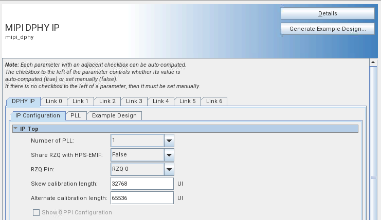
| Parameter Name | Description | Setting |
|---|---|---|
| Number of PLL | Set number of PLL to use for clock generation. The IP can use up to 2 PLLs to share among the different D-PHY links. The bit rates of the D-PHY links has to be the same to share a PLL. | 1 (default) or 2. |
| Share RZQ with HPS EMIF | Allow RZQ sharing with DDR4 or DDR5 HPS-EMIF IP. This parameter only applies to Agilex 5 devices | False (default) or True |
| RZQ Pin | Set RZQ pin location to use for the D-PHY IP. Pin 38 in one I/O bank is RZQ0 and pin 62 is RZQ1. Pin 38 reserves BYTE LOCATION 3, and pin 62 reserves BYTE LOCATION 5. |
RZQ0 (default) or RZQ1. (default for B18A devices.) |
| Skew calibration length | Length of initial skew calibration pattern automatically generated by D-PHY TX IP when SKEW_CAL_EN = 1. This is done automatically after the t INIT period. When SKEW_CAL_EN = 0, protocol IP is responsible to drive TxSkewCalHS to generate init skew sequence. SKEW_CAL_LEN is ignored by D-PHY RX IP. | 32768 (The default and the minimum.) |
| Alternate calibration length | Length of alternate calibration pattern automatically generated by D-PHY TX IP when ALT_CAL_EN = 1. This is done automatically after the init skew. When SKEW_CAL_EN = 0, protocol IP is responsible to drive TxAlTCalHS to generate alt cal sequence.ALT_CAL_LEN is ignored by D-PHY RX IP. | 65536 (The default and the minimum.) |
D-PHY IP PLL Tab
On the PLL tab, you configure the PLL settings such as core clock divider, PLL reference clock frequency, I/O standard selection, and VCO clock frequency.
Figure 7. D-PHY IP PLL Tab
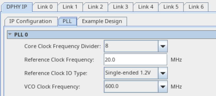
| Parameter Name | Description | Setting |
|---|---|---|
| Core clock frequency divider | Set core clock frequency divider to generate core clock from VCO output. MIPI only supports divided by 4 or 8. | 4 or 8. (Default value is 8.) |
| Reference clock frequency | PLL reference clock frequency. | 10MHz - 300MHz. (Default value is 20MHz.) |
| Reference clock I/O type | Reference Clock I/O standard. | Single Ended 1.2V, LVDS 1.2V Single Ended 1.1V, LVDS 1.1V . |
| Share Reference Clock I/O | Share PLL1 reference clock with PLL0. | True or False. (Default value is True.) |
| VCO Clock Frequency | Set the VCO clock frequency for PLL.
|
600 MHz - 1750 MHz. |