MIPI D-PHY IP User Guide: Agilex™ 3 and Agilex™ 5 FPGAs
ID
817561
Date
6/30/2025
Public
1. About the MIPI D-PHY IP
2. Configuring and Generating the MIPI D-PHY IP
3. MIPI D-PHY Interface Design Guidelines
4. Simulating the MIPI D-PHY IP
5. Validating the MIPI D-PHY IP
6. Debugging the MIPI-PHY IP
7. MIPI D-PHY Architecture
8. Interface Signals and Register Maps
9. Verification Test Plan
10. Document Revision History for the MIPI D-PHY IP User Guide
6.1. Creating a Simplified Design that Demonstrates the Same Problem
6.2. Evaluating FPGA Timing Problems
6.3. Determining if the Problem Exists in Previous Quartus Prime Versions
6.4. Determining if the Problem Exists in the Current Version of Software
6.5. Verifying the MIPI D-PHY IP Using the Signal Tap Logic Analyzer
6.6. Varying the Voltage
6.7. Operating at Lower Speed
6.8. Trying a Different PCB
8.2.1.1. IP_ID
8.2.1.2. IP_CAP
8.2.1.3. D0_CAP
8.2.1.4. DN_CAP
8.2.1.5. RX_CAP
8.2.1.6. TX_CAP
8.2.1.7. TX_PREAMBLE_LEN
8.2.1.8. D-PHY_CSR
8.2.1.9. TX_CLK_LANE_PS
8.2.1.10. RX_DLANE_ERR
8.2.1.11. SKEW_CAL_LEN_B0
8.2.1.12. SKEW_CAL_LEN_B1
8.2.1.13. SKEW_CAL_LEN_B2
8.2.1.14. SKEW_CAL_LEN_B3
8.2.1.15. ALT_CAL_LEN_B0
8.2.1.16. ALT_CAL_LEN_B1
8.2.1.17. ALT_CAL_LEN_B2
8.2.1.18. ALT_CAL_LEN_B3
8.2.1.19. CLK_CSR
8.2.1.20. CLK_STATUS
8.2.1.21. DLANE_CSR_0
8.2.1.22. DLANE_STATUS_0
8.2.1.23. RX_DLANE_DESKEW_DELAY_0
8.2.1.24. RX_DLANE_ERR_0
8.2.1.25. DLANE_CSR_1
8.2.1.26. DLANE_STATUS_1
8.2.1.27. RX_DLANE_DESKEW_DELAY_1
8.2.1.28. RX_DLANE_ERR_1
8.2.1.29. DLANE_CSR_2
8.2.1.30. DLANE_STATUS_2
8.2.1.31. RX_DLANE_DESKEW_DELAY_2
8.2.1.32. RX_DLANE_ERR_2
8.2.1.33. DLANE_CSR_3
8.2.1.34. DLANE_STATUS_3
8.2.1.35. RX_DLANE_DESKEW_DELAY_3
8.2.1.36. RX_DLANE_ERR_3
8.2.1.37. DLANE_CSR_4
8.2.1.38. DLANE_STATUS_4
8.2.1.39. RX_DLANE_DESKEW_DELAY_4
8.2.1.40. RX_DLANE_ERR_4
8.2.1.41. DLANE_CSR_5
8.2.1.42. DLANE_STATUS_5
8.2.1.43. RX_DLANE_DESKEW_DELAY_5
8.2.1.44. RX_DLANE_ERR_5
8.2.1.45. DLANE_CSR_6
8.2.1.46. DLANE_STATUS_6
8.2.1.47. RX_DLANE_DESKEW_DELAY_6
8.2.1.48. RX_DLANE_ERR_6
8.2.1.49. DLANE_CSR_7
8.2.1.50. DLANE_STATUS_7
8.2.1.51. RX_DLANE_DESKEW_DELAY_7
8.2.1.52. RX_DLANE_ERR_7
8.2.1.53. TX_LPX
8.2.1.54. TX_HS_EXIT
8.2.1.55. TX_LP_EXIT
8.2.1.56. TX_CLK_PREPARE
8.2.1.57. TX_CLK_ZERO
8.2.1.58. TX_CLK_POST
8.2.1.59. TX_CLK_PRE
8.2.1.60. TX_HS_PREPARE
8.2.1.61. TX_HS_ZERO
8.2.1.62. TX_HS_TRAIL
8.2.1.63. TX_INIT
8.2.1.64. TX_WAKE
8.2.1.65. RX_CLK_LOSS_DETECT
8.2.1.66. RX_CLK_SETTLE
8.2.1.67. RX_HS_SETTLE
8.2.1.68. RX_INIT
8.2.1.69. RX_CLK_POST
8.2.1.70. RX_CAL_REG_CTRL
8.2.1.71. RX_CAL_STATUS_D-PHY
8.2.1.72. RX_CAL_SKEW_W_START_MUX
8.2.1.73. RX_CAL_SKEW_W_END_MUX
8.2.1.74. RX_CAL_ALT_W_START_MUX
8.2.1.75. RX__CAL_ALT_W_END_MUX
8.2.1.76. RX_DESKEW_DELAY_MUX
8.2.1.77. RX_CAL_STATUS_LANE_MUX
8.2.1.78. PRBS_INIT_0
8.2.1.79. PRBS_INIT_1
8.2.1.80. PRBS_INIT_2
8.2.1.81. PRBS_INIT_3
8.2.1.82. PRBS_INIT_4
8.2.1.83. PRBS_INIT_5
8.2.1.84. PRBS_INIT_6
8.2.1.85. TX_TM_CONTROL
8.2.1.86. TX_MNL_IO_0
8.2.1.87. TX_MNL_D_LP_EN
8.2.1.88. RX_TM_CONTROL
8.2.2.1. TG_TOP_CTRL_0
8.2.2.2. TG_TOP_CTRL_1
8.2.2.3. TG_TOP_DONE
8.2.2.4. TG_TOP_FAIL
8.2.2.5. TG_TOP_TEST_EN
8.2.2.6. TG_TOP_TEST_LINK
8.2.2.7. TARGET_TEST_CNT
8.2.2.8. TCHK_CONTROL
8.2.2.9. TCHK_LINK_STATUS
8.2.2.10. HS_DONE_LANES
8.2.2.11. TCHK_LINK_ERR_STATUS
8.2.2.12. LANE_ERROR_SOT_LANES
8.2.2.13. CAL_ERROR_LANES
8.2.2.14. HS_ERR_LANES
8.2.2.15. HS_TEST_CNT
8.2.2.16. LPDT_TEST_CNT
8.2.2.17. TRIGGER_TEST_CNT
8.2.2.18. ULPS_TEST_CNT
8.2.2.19. TG_RX_OVRD_DATA_PAT
8.2.2.20. TG_RX_BIT_ERROR_CNT
8.2.2.21. TG_RX_HS_TXFER_CNT
8.2.2.22. TG_LINK_CONTROL
8.2.2.23. TG_INIT_CNT
8.2.2.24. TG_HS_LEN
8.2.2.25. TG_LP_LEN
8.2.2.26. TG_SKEW_CAL
8.2.2.27. TG_ALT_CAL
8.2.2.28. TG_PER_SKEW_CAL_LEN
8.2.2.29. TG_TEST_CNT
8.2.2.30. TG_OVRD_DATA_PAT
8.2.2.31. TG_TX_HS_TXFER_CNT
2.3. Generating the Design Example
An automated design example flow is available for the MIPI D-PHY IP.
You can generate a design example that matches the MIPI D-PHY IP that you require. You can use the design example to assist your evaluation, or as a starting point for your own system. For successful design example generation, you must enable at least one link by selecting for TX or RX implementation.
- Click Example Design tab and specify your parameters.
Figure 4. Example Design Tab
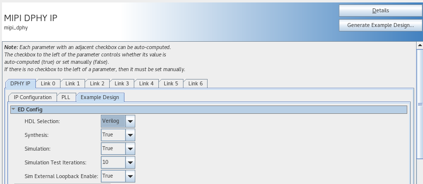
Table 3. Example Design Parameters Parameter Setting Description HDL Selection Verilog HDL or VHDL (default value is Verilog HDL). Hardware description language (HDL) selection. Synthesis True or False. (Default value is True.) Generate synthesis design example, which consists of: - D-PHY IP
- PPI traffic generator; 1 for each TX link.
- PPI pattern checker; 1 for each RX link.
- JTAG bridge to access CSR registers.
- Reset release IP.
- Interconnect blocks.
Simulation True or False. (Default value is True.) Generate simulation design example. Simulation Test Iterations 1-1023. (Default value is 10.) Number of test iteration. Sim External Loopback Enabled True or False. (Default value is True.) Generation simulation design example with external loopback. - Click Generate Example Designs to specify and generate the synthesis and simulation design example file sets that you can use to validate your MIPI D-PHY IP.