MIPI D-PHY IP User Guide: Agilex™ 3 and Agilex™ 5 FPGAs
ID
817561
Date
6/30/2025
Public
1. About the MIPI D-PHY IP
2. Configuring and Generating the MIPI D-PHY IP
3. MIPI D-PHY Interface Design Guidelines
4. Simulating the MIPI D-PHY IP
5. Validating the MIPI D-PHY IP
6. Debugging the MIPI-PHY IP
7. MIPI D-PHY Architecture
8. Interface Signals and Register Maps
9. Verification Test Plan
10. Document Revision History for the MIPI D-PHY IP User Guide
6.1. Creating a Simplified Design that Demonstrates the Same Problem
6.2. Evaluating FPGA Timing Problems
6.3. Determining if the Problem Exists in Previous Quartus Prime Versions
6.4. Determining if the Problem Exists in the Current Version of Software
6.5. Verifying the MIPI D-PHY IP Using the Signal Tap Logic Analyzer
6.6. Varying the Voltage
6.7. Operating at Lower Speed
6.8. Trying a Different PCB
8.2.1.1. IP_ID
8.2.1.2. IP_CAP
8.2.1.3. D0_CAP
8.2.1.4. DN_CAP
8.2.1.5. RX_CAP
8.2.1.6. TX_CAP
8.2.1.7. TX_PREAMBLE_LEN
8.2.1.8. D-PHY_CSR
8.2.1.9. TX_CLK_LANE_PS
8.2.1.10. RX_DLANE_ERR
8.2.1.11. SKEW_CAL_LEN_B0
8.2.1.12. SKEW_CAL_LEN_B1
8.2.1.13. SKEW_CAL_LEN_B2
8.2.1.14. SKEW_CAL_LEN_B3
8.2.1.15. ALT_CAL_LEN_B0
8.2.1.16. ALT_CAL_LEN_B1
8.2.1.17. ALT_CAL_LEN_B2
8.2.1.18. ALT_CAL_LEN_B3
8.2.1.19. CLK_CSR
8.2.1.20. CLK_STATUS
8.2.1.21. DLANE_CSR_0
8.2.1.22. DLANE_STATUS_0
8.2.1.23. RX_DLANE_DESKEW_DELAY_0
8.2.1.24. RX_DLANE_ERR_0
8.2.1.25. DLANE_CSR_1
8.2.1.26. DLANE_STATUS_1
8.2.1.27. RX_DLANE_DESKEW_DELAY_1
8.2.1.28. RX_DLANE_ERR_1
8.2.1.29. DLANE_CSR_2
8.2.1.30. DLANE_STATUS_2
8.2.1.31. RX_DLANE_DESKEW_DELAY_2
8.2.1.32. RX_DLANE_ERR_2
8.2.1.33. DLANE_CSR_3
8.2.1.34. DLANE_STATUS_3
8.2.1.35. RX_DLANE_DESKEW_DELAY_3
8.2.1.36. RX_DLANE_ERR_3
8.2.1.37. DLANE_CSR_4
8.2.1.38. DLANE_STATUS_4
8.2.1.39. RX_DLANE_DESKEW_DELAY_4
8.2.1.40. RX_DLANE_ERR_4
8.2.1.41. DLANE_CSR_5
8.2.1.42. DLANE_STATUS_5
8.2.1.43. RX_DLANE_DESKEW_DELAY_5
8.2.1.44. RX_DLANE_ERR_5
8.2.1.45. DLANE_CSR_6
8.2.1.46. DLANE_STATUS_6
8.2.1.47. RX_DLANE_DESKEW_DELAY_6
8.2.1.48. RX_DLANE_ERR_6
8.2.1.49. DLANE_CSR_7
8.2.1.50. DLANE_STATUS_7
8.2.1.51. RX_DLANE_DESKEW_DELAY_7
8.2.1.52. RX_DLANE_ERR_7
8.2.1.53. TX_LPX
8.2.1.54. TX_HS_EXIT
8.2.1.55. TX_LP_EXIT
8.2.1.56. TX_CLK_PREPARE
8.2.1.57. TX_CLK_ZERO
8.2.1.58. TX_CLK_POST
8.2.1.59. TX_CLK_PRE
8.2.1.60. TX_HS_PREPARE
8.2.1.61. TX_HS_ZERO
8.2.1.62. TX_HS_TRAIL
8.2.1.63. TX_INIT
8.2.1.64. TX_WAKE
8.2.1.65. RX_CLK_LOSS_DETECT
8.2.1.66. RX_CLK_SETTLE
8.2.1.67. RX_HS_SETTLE
8.2.1.68. RX_INIT
8.2.1.69. RX_CLK_POST
8.2.1.70. RX_CAL_REG_CTRL
8.2.1.71. RX_CAL_STATUS_D-PHY
8.2.1.72. RX_CAL_SKEW_W_START_MUX
8.2.1.73. RX_CAL_SKEW_W_END_MUX
8.2.1.74. RX_CAL_ALT_W_START_MUX
8.2.1.75. RX__CAL_ALT_W_END_MUX
8.2.1.76. RX_DESKEW_DELAY_MUX
8.2.1.77. RX_CAL_STATUS_LANE_MUX
8.2.1.78. PRBS_INIT_0
8.2.1.79. PRBS_INIT_1
8.2.1.80. PRBS_INIT_2
8.2.1.81. PRBS_INIT_3
8.2.1.82. PRBS_INIT_4
8.2.1.83. PRBS_INIT_5
8.2.1.84. PRBS_INIT_6
8.2.1.85. TX_TM_CONTROL
8.2.1.86. TX_MNL_IO_0
8.2.1.87. TX_MNL_D_LP_EN
8.2.1.88. RX_TM_CONTROL
8.2.2.1. TG_TOP_CTRL_0
8.2.2.2. TG_TOP_CTRL_1
8.2.2.3. TG_TOP_DONE
8.2.2.4. TG_TOP_FAIL
8.2.2.5. TG_TOP_TEST_EN
8.2.2.6. TG_TOP_TEST_LINK
8.2.2.7. TARGET_TEST_CNT
8.2.2.8. TCHK_CONTROL
8.2.2.9. TCHK_LINK_STATUS
8.2.2.10. HS_DONE_LANES
8.2.2.11. TCHK_LINK_ERR_STATUS
8.2.2.12. LANE_ERROR_SOT_LANES
8.2.2.13. CAL_ERROR_LANES
8.2.2.14. HS_ERR_LANES
8.2.2.15. HS_TEST_CNT
8.2.2.16. LPDT_TEST_CNT
8.2.2.17. TRIGGER_TEST_CNT
8.2.2.18. ULPS_TEST_CNT
8.2.2.19. TG_RX_OVRD_DATA_PAT
8.2.2.20. TG_RX_BIT_ERROR_CNT
8.2.2.21. TG_RX_HS_TXFER_CNT
8.2.2.22. TG_LINK_CONTROL
8.2.2.23. TG_INIT_CNT
8.2.2.24. TG_HS_LEN
8.2.2.25. TG_LP_LEN
8.2.2.26. TG_SKEW_CAL
8.2.2.27. TG_ALT_CAL
8.2.2.28. TG_PER_SKEW_CAL_LEN
8.2.2.29. TG_TEST_CNT
8.2.2.30. TG_OVRD_DATA_PAT
8.2.2.31. TG_TX_HS_TXFER_CNT
7. MIPI D-PHY Architecture
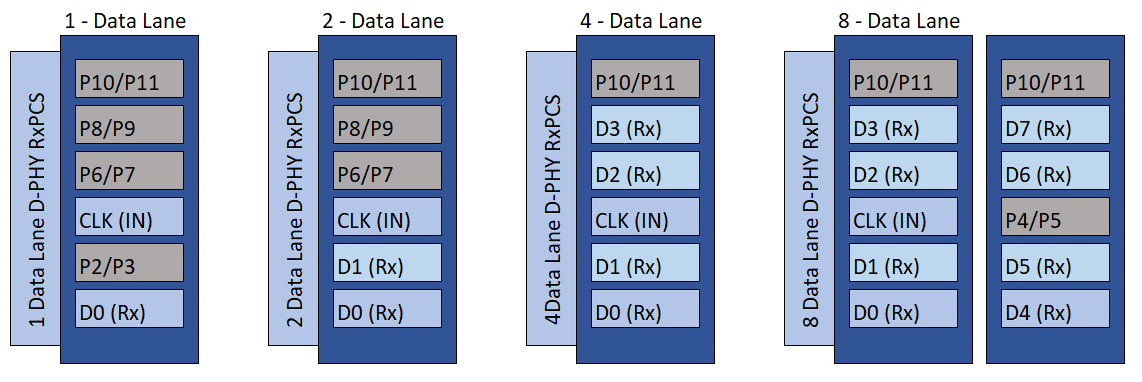
The Agilex™ 3 and Agilex™ 5 devices implement the MIPI D-PHY IP through HSIO banks. Each HSIO bank consists of 8 byte blocks to support MIPI D-PHY IP. However, one byte blocks is reserved for RZQ calibration and reference clock. Therefore the maximum MIPI D-PHY interfaces that a single HSIO bank can support is up to 7 interfaces (subject to D-PHY lanes configuration). Both the Agilex™ 3 and Agilex™ 5 devices offer a native D-PHY interface that allows direct point-to-point connection between the D-PHY transmitter and D-PHY receiver without any passive circuitry or third-party component in between. Each interface can support 1, 2, 4, or 8 data lanes plus 1 clock lane.
Figure 21. MIPI D-PHY IP TX Data and Clock Lane PlacementThe figure shows each interface has prefixed data lane and clock lane placement. Refer to the MIPI D-PHY Interface Implementation section to understand the implementation and how to identify the physical pin placement.
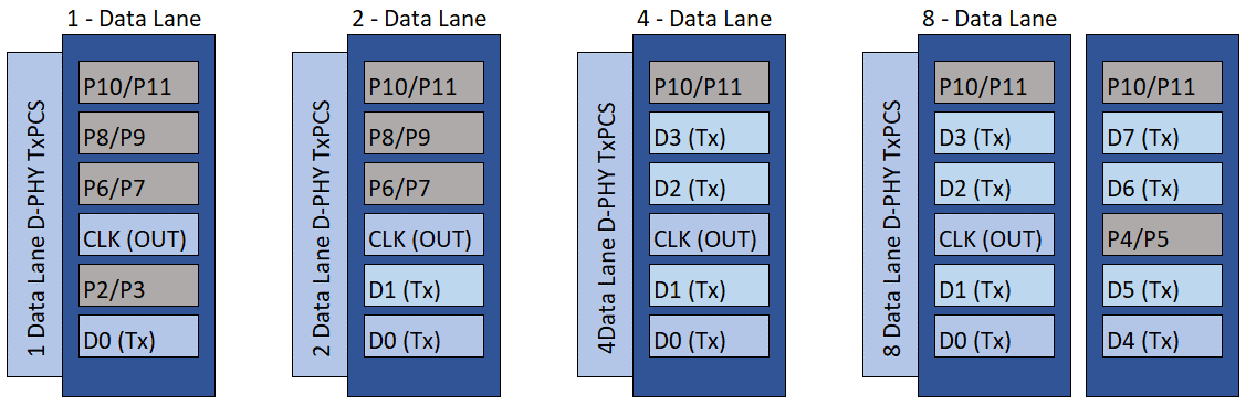
Figure 22. MIPI D-PHY IP RX Data and Clock Lane Placement