External Memory Interfaces Agilex™ 7 M-Series FPGA IP User Guide
A newer version of this document is available. Customers should click here to go to the newest version.
- 4.1.2. s0_axi4_clock_out for Agilex 7 M-Series External Memory Interfaces (EMIF) IP - DDR4 Component
- 4.3.2. s0_axi4_clock_out for Agilex 7 M-Series External Memory Interfaces (EMIF) IP - DDR5 Component
11.10.2.1. Verifying High-Level Configuration
Memory Device
Verify that you select the correct memory Number of Channels, Data DQ Width, Die Density, and CS Width for the memory configuration used. Inaccurate information can result in calibration failure or traffic failure.
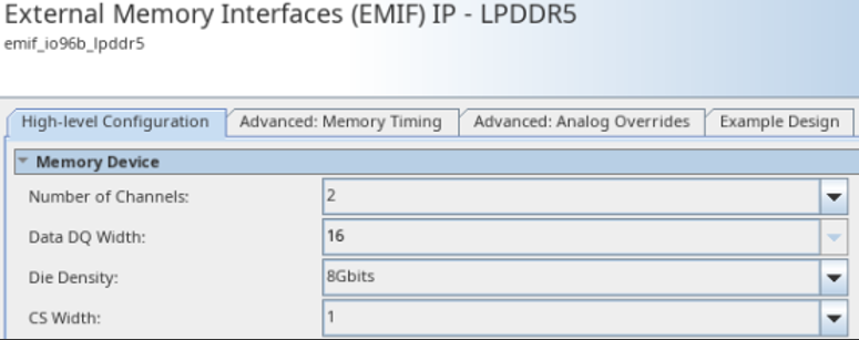
The example below shows memory parameterization based on the Agilex™ 7 FPGA M-Series Development Kit targeting an MT62F512M32D2 LPDDR5 EMIF configuration.
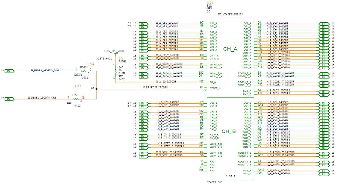
- Number of Channels: 2 (Dedicated A/C pins for each channel.)
- Data DQ Width: 16 (DQ pins per memory channel.)
- Die Density: 8 Gbits (Select capacity of each memory die <in Gbits>, not total memory density per package.)
- CS width: 1 (Above topology is single-rank per channel. MT62F512M32D2 supports single-rank per die per channel based on the die organization in memory component datasheet.)
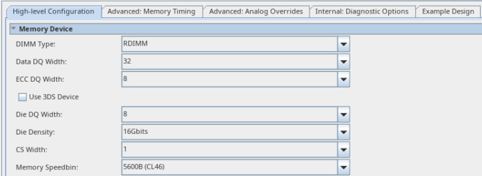
Another example showing a configuration based on Agilex™ 7 FPGA M-Series Development Kit targeting DDR5 RDIMM is shown below.
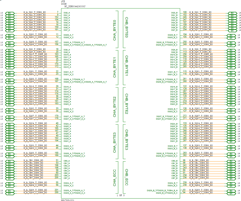

- DIMM Type: RDIMM.
- Data DQ Width: 32 (DQ pins per memory channel, used for data.)
- ECC DQ Width: 8 (Additional DQ pins per channel, used for ECC.)
- Die DQ Width: 8 (Numbers of DQ pins in each die. For dual-die package, select width of each die, not width of full package.)
- Die Density: 16Gbits (Select capacity of each memory die <in Gbits> per channel per die. For dual-die package, this is the density of each die, not the density of the full package.)
- CS width: 1 (Above topology is Single Rank per channel.)
Pin Swizzle map
The Quartus® Prime software uses fixed pin placement for each supported memory standard, as described in the Product Architecture chapter. Do not change pin placement using a .qsf assignment or the pin planner if you need to swap the DQ pins within a DQS group or swap the DQS group within a channel or interface. You may encounter fitter errors if you enter incorrect pin locations for the EMIF interface. The example below shows fitter error for LPDDR5 protocol when an incorrect pin location is used.
Error (175001): The Fitter cannot place 1 BYTE, which is within Generic Component ed_synth_emif_io96b_lpddr5_0.
The Pin Swizzle Map allows you to inform the EMIF IP about the ordering of the physical connections of each DQ pin on the memory component to the FPGA. Incorrect information entered in the pin swizzle map may cause calibration errors.
Refer to the External Memory Interfaces Agilex™ 7 M-Series FPGA IP Design Example User Guide for details on configuring DQ pin swizzling.

Pin Swizzle Map for Component Interfaces
For component type interfaces, you must match the net name in the schematic to the index of default pin placements, to determine the pin swizzling specification.
Consider the example in the table below, which represents DQS group 1 for channel 1 on the LPDDR5 component interface on the Agilex™ 7 FPGA M-Series Development Kit with MT62F512M32D2 memory.
| Lane | Pin | Pin Index | Default Pin Placement | Net Name in Schematic | Swizzling index |
|---|---|---|---|---|---|
| BL6 | K57 | 83 | MEM_1_MEM_DQ [7] | MEM_1_MEM_DQ [14] | 14 |
| L56 | 82 | MEM_1_MEM_DQ [6] | MEM_1_MEM_DQ [12] | 12 | |
| H57 | 81 | MEM_1_MEM_DQ [5] | MEM_1_MEM_DQ [13] | 13 | |
| G56 | 80 | MEM_1_MEM_DQ [4] | MEM_1_MEM_DQ [11] | 11 | |
| K55 | 79 | ||||
| L54 | 78 | MEM_1_MEM_DM_N [0] | MEM_1_MEM_DM_N [1] | ||
| H55 | 77 | MEM_1_MEM_RDQS_C [0] | MEM_1_MEM_RDQS_C [1] | ||
| G54 | 76 | MEM_1_MEM_RDQS_T [0] | MEM_1_MEM_RDQS_T [1] | ||
| K53 | 75 | MEM_1_MEM_DQ [3] | MEM_1_MEM_DQ [9] | 9 | |
| L52 | 74 | MEM_1_MEM_DQ [2] | MEM_1_MEM_DQ [10] | 10 | |
| H53 | 73 | MEM_1_MEM_DQ [1] | MEM_1_MEM_DQ [8] | 8 | |
| G52 | 72 | MEM_1_MEM_DQ [0] | MEM_1_MEM_DQ [15] | 15 |
For this specific group, the correct pin swizzling specification is:
PIN_SWIZZLE_CH1_DQS1 = 15,8,10,9,11,13,12,14;
The sample below shows pin swizzle map parameters based on Agilex™ 7 M-Series Development Kit targeting LPDDR5 EMIF. All parameters must be added in the Pin Swizzle Map entry in a single line separated by semi-colons.
BYTE_SWIZZLE_CH0=1,0,X,X,X,X,X,X;
PIN_SWIZZLE_CH0_DQS1=9,11,8,10,13,15,14,12;
PIN_SWIZZLE_CH0_DQS0=6,7,4,5,0,3,2,1;
BYTE_SWIZZLE_CH1=X,X,X,X,X,X,1,0;
PIN_SWIZZLE_CH1_DQS1=15,8,10,9,11,13,12,14;
PIN_SWIZZLE_CH1_DQS0=7,6,4,5,3,2,1,0;
Pin Swizzle Map for DIMM interface
For DIMM topologies, you must incorporate the component-to-module DQ map (refer to the memory vendor's datasheet), to determine the pin swizzling specification for the DIMM interface.
Consider the example in the table below, which represents DQS group 0 for channel 0 on the DDR5 RDIMM interface on the Agilex™ 7 FPGA M-Series Development Kit with MTC10F1084S1RC56BG1 DDR5 RDIMM memory.
| Information From Dev Kit Schematic | Information from Memory Vendor Data Sheet (Component-to-Module DQ Map) | |||||
|---|---|---|---|---|---|---|
| Lane | Pin | Pin Index | Net Name in Schematic | Component Ref Number | Module DQ | Component DQ |
| BL6 | FV23 | 83 | M_A_DQ5_T_DDR5_RD | U4 | 5A | 7 |
| FU24 | 82 | M_A_DQ6_T_DDR5_RD | 6A | 6 | ||
| FY23 | 81 | M_A_DQ7_T_DDR5_RD | 7A | 5 | ||
| GA24 | 80 | M_A_DQ4_T_DDR5_RD | 4A | 4 | ||
| FU26 | 79 | M_A_DQS5_C_DDR5_RD | ||||
| FV25 | 78 | M_A_DQS5_T_DDR5_RD | ||||
| GA26 | 77 | M_A_DQS0_C_DDR5_RD | ||||
| FY25 | 76 | M_A_DQS0_T_DDR5_RD | ||||
| FV27 | 75 | M_A_DQ1_T_DDR5_RD | 1A | 1 | ||
| FU28 | 74 | M_A_DQ2_T_DDR5_RD | 2A | 0 | ||
| FY27 | 73 | M_A_DQ3_T_DDR5_RD | 3A | 3 | ||
| GA28 | 72 | M_A_DQ0_T_DDR5_RD | 0A | 2 | ||
For this specific group, the correct pin swizzling specification is:
PIN_SWIZZLE_CH0_DQS0 = 2,3,0,1,4,5,6,7;
(Note that the PIN_SWIZZLE_CH0_DQS0 = 0,3,2,1,4,7,6,5; specification would be incorrect. Pin swizzling specifications can be different when using different DIMMs.)
The example below shows the full Pin Swizzle Map parameters based on an Agilex™ 7 M-Series development kit targeting an MTC10F1084S1RC56BG1 DDR5 RDIMM memory interface. All parameters must be added in the Pin Swizzle Map entry in a single line separated by semi-colons. Ensure that the DQ pin swizzles are based on the component DQ index and not the Module/DIMM DQ index; inaccurate swizzling will result in calibration failure.
BYTE_SWIZZLE_CH0=X,ECC,2,1,X,X,0,3;
PIN_SWIZZLE_CH0_DQS0=2,3,0,1,4,5,6,7;
PIN_SWIZZLE_CH0_DQS1=8,11,10,9,13,15,12,14;
PIN_SWIZZLE_CH0_DQS2=18,17,16,19,20,23,21,22;
PIN_SWIZZLE_CH0_DQS3=27,24,25,26,29,30,28,31;
PIN_SWIZZLE_CH0_ECC=2,1,0,3,4,7,6,5;
BYTE_SWIZZLE_CH1=0,1,X,X,3,2,ECC,X;
PIN_SWIZZLE_CH1_DQS0=0,1,3,2,4,5,7,6;
PIN_SWIZZLE_CH1_DQS1=8,10,9,11,12,13,15,14;
PIN_SWIZZLE_CH1_DQS2=19,16,18,17,21,22,23,20;
PIN_SWIZZLE_CH1_DQS3=25,26,24,27,31,28,30,29;
PIN_SWIZZLE_CH1_ECC=6,5,7,4,0,3,2,1;