External Memory Interfaces Agilex™ 7 M-Series FPGA IP User Guide
A newer version of this document is available. Customers should click here to go to the newest version.
- 4.1.2. s0_axi4_clock_out for Agilex 7 M-Series External Memory Interfaces (EMIF) IP - DDR4 Component
- 4.3.2. s0_axi4_clock_out for Agilex 7 M-Series External Memory Interfaces (EMIF) IP - DDR5 Component
3.1.3.1. I/O Byte Lane Organization in Different Agilex™ 7 M-Series Devices
R47A and R47B packages have the same byte lane configuration, and differ in the available transceiver tiles. R31B is a package that enables design migration from Agilex™ 7 I-Series to Agilex™ 7 M-Series devices that share this same package.
The following figures show the I/O byte lanes organization and availability across the different I/O Banks for each package.
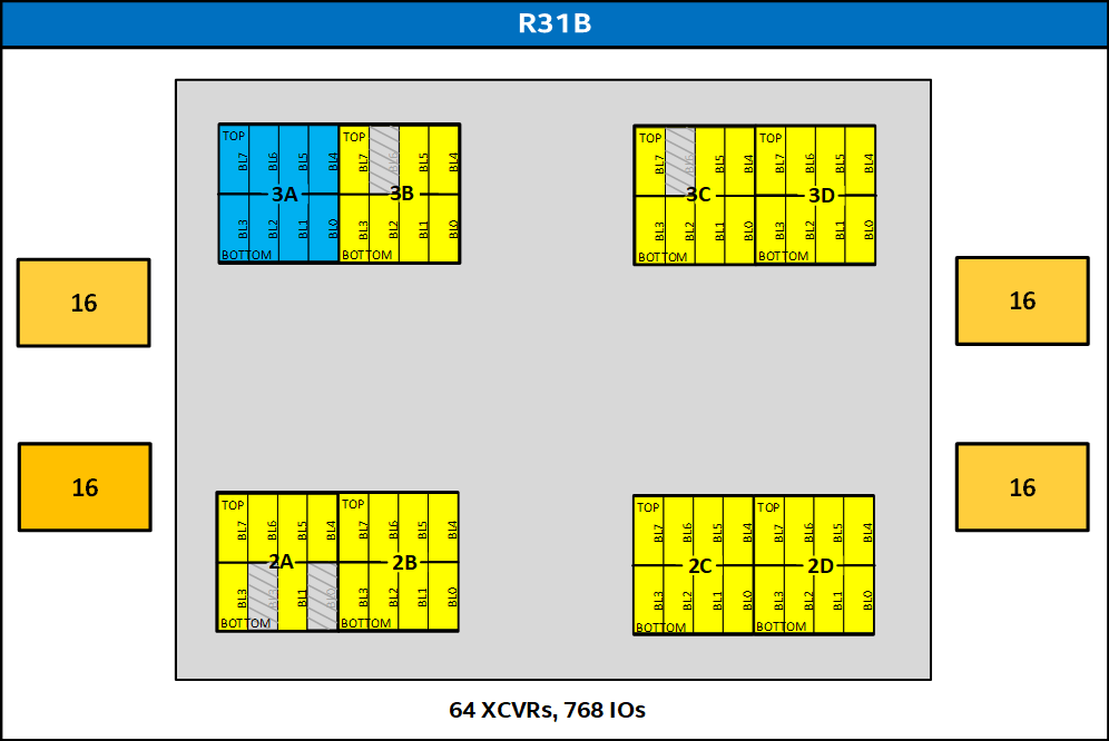
R31B Package
In bank 3B and 3C top sub-bank, byte lane #6 is not available; in bank 2A bottom sub-bank, byte lanes #0 and #3 are not available. This affects the maximum number of external memory interfaces per device.
For more information, refer to Maximum Number of DDR4 Interfaces, Maximum Number of DDR5 Interfaces, and Maximum Number of LPDDR5 Interfaces.
R47A Package
All byte lanes are available in all banks. For information on the maximum number of interfaces for a given protocol, refer to Maximum Number of DDR4 Interfaces, Maximum Number of DDR5 Interfaces, and Maximum Number of LPDDR5 Interfaces.

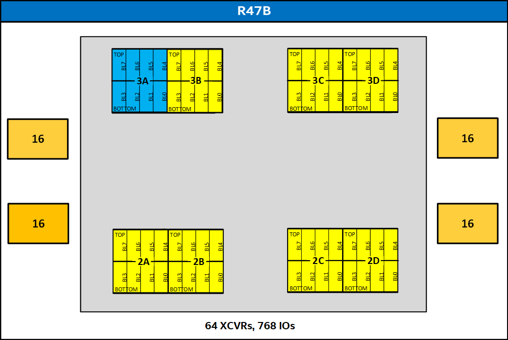
R47B Package
All byte lanes are available in all banks. For information on the maximum number of interfaces for a given protocol, refer to Maximum Number of DDR4 Interfaces, Maximum Number of DDR5 Interfaces, and Maximum Number of LPDDR5 Interfaces.