F-Tile Ethernet Intel® FPGA Hard IP Design Example User Guide
ID
683804
Date
12/19/2022
Public
A newer version of this document is available. Customers should click here to go to the newest version.
1. Quick Start Guide
2. Design Example: Single IP Core Instantiation
3. Design Example: Single IP Core Instantiation with Precision Time Protocol
4. Design Example: Single IP Core Instantiation with Auto-Negotiation and Link Training
5. Design Example: Multiple IP Core Instantiation
6. F-Tile Ethernet Intel® FPGA Hard IP Design Example User Guide Archives
7. Document Revision History for the F-Tile Ethernet Intel FPGA Hard IP Design Example User Guide
1.5. Compiling and Configuring the Design Example in Hardware
To compile the hardware design example and configure it on your Intel device, follow these steps:
- Ensure hardware design example generation is complete.
- In the Intel® Quartus® Prime Pro Edition software, navigate to the Intel® Quartus® Prime project directory eth_f_0_example_design/hardware_test_design/.
- Open the Intel® Quartus® Prime project:
quartus eth_f_hw.qpf & - On the Processing menu, click Start Compilation.
- After successful compilation, a .sof file is available in <design_example_directory>/hardware_test_design/output_files.
- Connect the Agilex I-Series Transceiver-SoC Development Kit to the host computer.
- Launch the Clock Controller application, which is part of the development kit.
Figure 8. Clock Controller
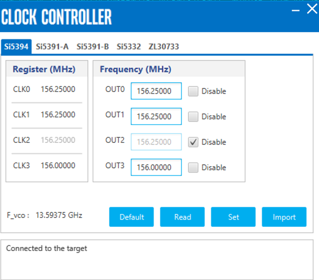 Set new frequencies for the design example as following:
- Si5394 (U118), OUT3: Set to the value of i_refclk2pll 2 as 156.25MHz.
- On the Tools menu, click Programmer.
- In the Programmer, click Hardware Setup.
- Select a programming device.
- Select and add the Development Kit to which your Intel® Quartus® Prime Pro Edition session can connect.
- Ensure that Mode is set to JTAG.
- Select the device and click Add Device. The Programmer displays a block diagram of the connections between the devices on your board.
- In the row with your .sof, check the Program/Configure box for the .sof file.
- Click Start.
Note: If the System PLL fails to lock when the i_refclk2pll frequency is greater than 156.25MHz, please refer to the steps specified in Why do F-tile Reference and System PLL clocks Intel® FPGA IP fail to lock at specific frequencies? to resolve the issue.
2 The Clock Control GUI application cannot drive all the frequencies.