AN 522: Implementing Bus LVDS Interface in Supported Intel® FPGA Device Families
ID
683803
Date
7/31/2018
Public
Design Example Guidelines for All Supported Devices Except Intel® Arria® 10, Intel® Cyclone® 10 GX, and Intel® MAX® 10
These steps are applicable to all supported devices except Intel® Arria® 10, Intel® Cyclone® 10 GX, and Intel® MAX® 10. Ensure that you use the ALTIOBUF IP core.
- Create an ALTIOBUF IP core that can support a bidirectional input and output buffer:
- Instantiate the ALTIOBUF IP core.
- Configure the module As a bidirectional buffer.
- In What is the number of buffers to be instantiated, enter 1.
- Turn on Use differential mode.
- Connect the modules and the input and output ports as shown in the following figure:
Figure 12. Input and Output Ports Connection Example for All Supported Devices Except Intel® Arria® 10, Intel® Cyclone® 10 GX, and Intel® MAX® 10 Devices
- In the Assignment Editor, assign the relevant I/O standard as shown in the following figure according to your device. You can also set the current strength and slew rate options. Otherwise, the Intel® Quartus® Prime software assumes the default settings.
- Intel® Cyclone® 10 LP, Cyclone® IV, Cyclone® III, and Cyclone® III LS devices—BLVDS I/O standard to the bidirectional p and n pins as shown in the following figure.
- Stratix® V, Stratix® IV, Stratix® III, Arria® V, Arria® II, and Cyclone® V devices—Differential SSTL-2 Class I or Class II I/O standard.
Figure 13. BLVDS I/O Assignment in the Intel® Quartus® Prime Assignment Editor
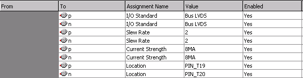
Note: You can manually assign both the p and n pin locations for each supported device with the Assignment Editor. For the supported devices and the pins you can manually assign, refer to the related information. - Compile and perform functional simulation with the ModelSim* - Intel® FPGA Edition software.
Figure 14. Example of Functional Simulation ResultsWhen the oe signal is asserted, the BLVDS is in write operation mode. When the oe signal is deasserted, the BLVDS is in read operation mode.
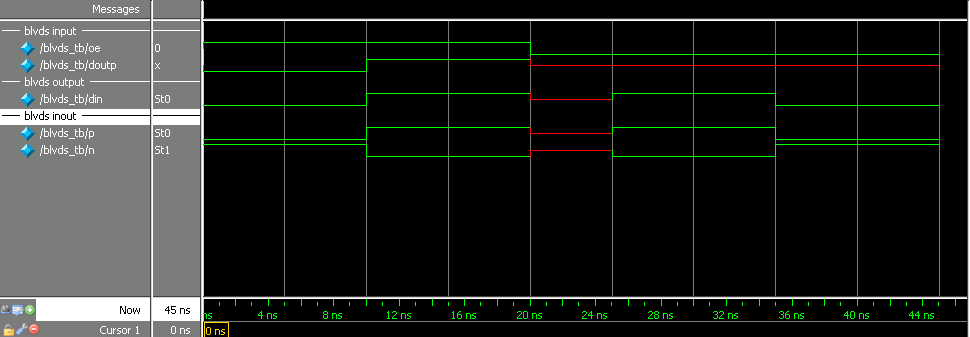
Note: For simulation using Verilog HDL, you can use the blvds_tb.v testbench, which is included in the respective design example.