Multi Channel DMA for PCI Express* Intel® FPGA IP Design Example User Guide
ID
683517
Date
12/01/2021
Public
A newer version of this document is available. Customers should click here to go to the newest version.
2.3.1.1.1. Simulation Result
Testbench writes 4 KB of incrementing pattern to on-chip memory and read back via Avalon-MM PIO interface. This design example testbench doesn’t simulate H2D/D2H data movers.
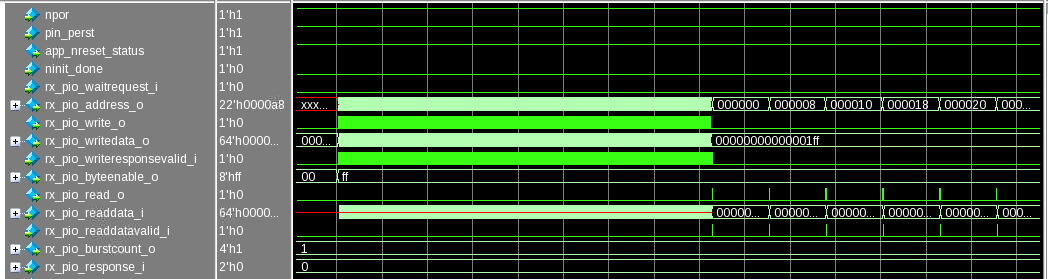
Figure 2. Simulation Log
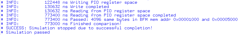
Figure 3. Simulation Waveform